

Packaging for 3D/2.5D IC integration
As IC technology advances, the need for more reliable and efficient packaging solutions is becoming increasingly important. With the emergence of 3D/2.5D IC integration, the complexity of semiconductor packaging has increased significantly. 3D/2.5D IC integration involves stacking multiple layers of ICs together in a single package. The layers are connected using through-silicon vias (TSVs) and microbumps. This type of integration provides a more efficient and cost effective solution compared to traditional 2D packaging. However, the complexity of 3D/2.5D IC integration requires more advanced semiconductor packaging solutions.
When packaging 3D/2.5D ICs, the semiconductor packaging material must be able to handle the increased complexity and provide reliable electrical connections between the layers. The materials must also be able to withstand the extreme temperatures and pressures that occur during manufacturing and operation. Additionally, the semiconductor packaging must be able to handle the high density of interconnects between the layers.
At Nanosystems JP, we provide a range of high-performance 3D/2.5D IC packaging fabrication services to meet the most demanding requirements. Allowing highest levels of performance and reliability, enabling customers to achieve the highest levels of design, power and thermal efficiency.

Typical Process Flow

TSV in a Silicon wafer
2. Backside processing

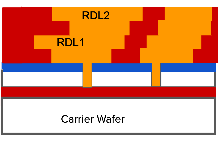
2. Backside RDL
3.UBM and C4 Bumping

3.Frontside processing

2. Frontside UBM & Cu post or Pillars fabrication
Chip | Wafer

3. Package substrate

4. Under filling and molding


If you have any questions about our Packaging for 3D/2.5D IC integration fabrication process, please don't hesitate to contact us.