Thin Film Deposition & Coating Services
At Nanosystems JP Inc., we offer PVD, CVD, ALD, MBE, PECVD, ion plating, optical coatings, and roll-to-roll deposition. Substrates from small wafers up to 500×600 mm rectangular panels for sputtering, evaporation, and PECVD (ALD and MBE run on wafer formats).
targets available
method families
size (mm)
range
Lift-Off Patterning
PVD sputtering and e-beam evaporation are the deposition methods used in lift-off patterning flows. We offer the full lift-off service - resist, exposure, PVD deposition, and solvent strip - for Au, Pt, TiN, and AuSn multi-layer stacks.
Every deposition method -
one foundry
Most devices need multiple deposition steps, sputtered metal contacts, PECVD dielectric insulation, ALD gate oxide, and MBE epitaxial growth can all be required in the same device. All of these are managed within a single project by a dedicated project manager.
Sputtering, E-beam & Thermal Evaporation
PVD is the backbone of electrode metallization, barrier layer deposition, and functional thin film formation. At Nanosystems JP Inc., we offer over 100 sputtering targets.
Most versatile PVD method. Metals, alloys, ceramics, and transparent conductors. Excellent film uniformity across large substrates. Low substrate temperature.
In-situ reactive gas forms compound films during deposition. Nitrides, oxides, and transparent conductors grown in a single step.
Specialist deposition of functional piezoelectric and ferroelectric thin films. Optimized crystallographic texture for maximum coupling coefficient.
High-purity metal films with low contamination. Excellent for liftoff processing. AuSn solder deposition for UBM flip-chip packaging.
Ion-assisted deposition combines vacuum evaporation with ion bombardment. Outstanding adhesion, density, and hardness. Optical coatings and hard wear layers.
Thermal oxide in an atmospheric furnace: dry oxidation 100-300 nm, wet oxidation 300 nm to 5 µm, wafers to 150 mm in batches of up to 80; thicker SiO₂ by PECVD or TEOS. Low defect density, excellent electrical isolation, and high interface quality for MOS structures.
At Nanosystems JP Inc., we offer deposition
from single chips to 500×600mm panels
Circular wafers and large rectangular substrates are both supported for sputtering, evaporation, and PECVD. Moving from wafer prototypes to panel production is managed as one project by your dedicated project manager, with route-specific process transfer confirmed at engineering review.
(Si, GaAs, SiC...)
glass / polymer panel
(angstroms to microns)
lots available
PECVD, LPCVD & LTPS
CVD methods grow films from gas-phase precursors, enabling conformal coverage of complex 3D structures, trench sidewalls, via liners, and MEMS cavities, that PVD cannot reach. PECVD operates at low temperature, compatible with completed device structures and flexible substrates. LPCVD delivers high-quality polycrystalline silicon, silicon nitride, and deposited oxide films (thermal oxide is grown separately by oxidation).
Low-temperature dielectric and semiconductor film deposition. RF plasma activates precursors below 400°C, compatible with BEOL processing and polymer substrates.
Low-temperature, low-stress SiN specially optimized for optical waveguide applications. Tunable refractive index and stress. Minimal absorption for waveguide propagation loss.
High-temperature, high-quality films with superior step coverage and uniformity. The standard for polysilicon gates, sacrificial layers, and deposited oxide liners in MEMS and semiconductor devices.
Crystalline silicon at low process temperatures. Enables TFT backplanes for displays and sensors on glass. Higher carrier mobility than amorphous silicon.
Hard, chemically inert carbon coating by PECVD. Extreme hardness, wear resistance, and low friction. Applied to MEMS wear surfaces, cutting tools, and biomedical implants.
N-doped, P-doped, and undoped a-Si:H. Used in thin-film solar cells, flat-panel detectors, TFTs, and as sacrificial layers in MEMS surface micromachining.
ALD, Sub-nm Precision,
Near-ideal Conformality
ALD uses sequential, self-limiting surface reactions. Growth per cycle depends on the material and process and is commonly a fraction of a monolayer, which gives three properties that are hard to reach with other methods: sub-nanometer thickness control, near-ideal step coverage into deep trenches and vias on qualified geometries, and dense, continuous films. These make ALD the method of choice for gate dielectrics, passivation layers on compound semiconductors, and moisture barrier coatings.
Most widely deposited ALD material. Gate dielectric for GaN HEMTs, passivation for GaAs/InP surfaces, moisture barrier for OLED displays and flexible electronics.
Conformal insulating layers for MEMS capacitors, via liners, and gate dielectrics. Superior step coverage vs PECVD into deep trenches and aspect ratios >10:1.
High refractive index optical coatings, photocatalytic surfaces, and high-k dielectric applications. Used in optical interference filters and anti-reflection systems.
High-k gate dielectric for advanced transistor nodes and DRAM capacitor dielectrics. Chemical stability and high dielectric constant (ε≈25) make it a key high-k material.
Near-ideal conformality into 3D structures (a fraction of a monolayer per self-limiting cycle). Sub-nm thickness control. Dense, continuous films. Low process temperature (80-300°C). Ultra-thin (<5nm) layers with defined composition.
GaN HEMT gate dielectric, GaAs/InP surface passivation, high-k MOSFET gate, MEMS wear coating, OLED encapsulation, TSV liner, memory capacitor dielectric.
MBE & Epitaxial Growth
MBE is the highest-precision deposition technique, atoms are delivered one layer at a time under ultra-high vacuum with real-time RHEED monitoring of crystal growth. This gives atomically sharp heterointerfaces, precise doping profiles, and strain-engineered quantum wells that are impossible to achieve by any other method. Essential for III-V photonic and power devices, and for research-grade quantum structures.
GaN and AlGaN epilayer growth for HEMT, LED, and power device structures. Precise control of Al composition, doping, and interface quality. MOCVD or MBE routes available.
Aluminum nitride epitaxial layers for deep-UV LEDs, SAW/BAW resonators, and AlGaN/GaN HEMT buffer layers. High crystalline quality on SiC and Si substrates.
Ion-beam assisted evaporation for high-quality optical coatings. Dense, hard, and stress-controlled films with precisely controlled refractive index and low scatter.
Roll-to-Roll Film &
Foil Deposition
Roll-to-roll deposition is our unique capability for large-area, flexible, and high-volume coating on continuous web substrates. Metal foils and polymer films pass through the deposition zone continuously, enabling cost-effective production of transparent electrodes, battery anodes, flexible sensors, and solar cell precursors at scales no batch wafer system can match.
Deposition on PET, Polyimide (Kapton), and Polycarbonate films. Sputtered ITO for flexible touch screens. Metal coatings for flexible sensors and heaters.
Coating on aluminum, copper, and steel foils. Silicon (amorphous) on copper foil as anode material for lithium-ion batteries, a growing market for flexible energy storage.
Metals, alloys, transparent conductors, oxides, nitrides and carbon films by sputtering, reactive sputtering and evaporation on continuous web. Pick any of these in the material library above to see its full route list.
Explore by material
Search by element, compound, or application, or pick an element from the periodic table to see the films that contain it. Each entry lists the deposition routes we run for it.
Every film we deposit -
method and application
This is the full material list from our live capabilities. If you don't see your material, contact us, we can often accommodate custom targets and precursors.
| Category | Materials | Method | Key Applications |
|---|---|---|---|
| Standard Metals | AlAuAgPtCrCuNiRuIrZrTaWRhRe |
Sputtering / E-beam / Thermal | Contacts, electrodes, interconnects, seed layers, hard masks |
| Barrier & Adhesion Layers | TiNTaNTiWSiNTiTiO₂ |
Reactive sputtering | Cu diffusion barrier, adhesion promotion, BEOL metallization |
| Piezoelectric Films | PZTKNNAlNKTN SIROF (electrode coating)LiPON (solid electrolyte) |
RF magnetron sputtering | MEMS actuators, BAW resonators, energy harvesters, solid-state batteries |
| Transparent Conductors | ITOAZOGZO |
Reactive sputtering / R2R | Touch panels, solar cells, OLED anodes, flexible electronics |
| ALD Oxides | Al₂O₃SiO₂TiO₂ZrO₂ |
ALD | Gate dielectric, GaN passivation, OLED barrier, TSV liner, high-k |
| CVD Dielectrics | SiO₂SiNSiONTEOSPSGNSGLTO |
PECVD / LPCVD | Interlayer dielectric, isolation, passivation, etch mask, waveguide cladding |
| CVD Silicon | Poly-Sia-Sia-Si:H (N/P/undoped)LTPS |
LPCVD / PECVD | MEMS sacrificial layer, gate material, TFT, photovoltaic, Li battery anode |
| Optical Coatings | MgF₂Ta₂O₅Al₂O₃ |
IBAD / ion plating | Anti-reflection, HR mirrors, bandpass filters, AR coatings for optics |
| Epitaxial III-N | GaNAlNAlGaNInGaN |
MBE / MOCVD | HEMT, LED, deep-UV LED, laser, power device epilayers |
| AuSn Solder | AuSn (80/20)UBM stack |
Thermal / E-beam (layered) | Flip-chip bonding, hermetic sealing, die attach for PIC/photonics |
| DLC & Carbon | DLCa-C:Hta-C |
PECVD | MEMS wear layers, hard coatings, tribological films, biomedical |
| Specialty Films | SiRiNLiPON (solid electrolyte)Thermal SiO₂ |
Sputtering / Thermal oxidation | Waveguide, solid-state battery electrolyte, MOS gate quality SiO₂ |
Industries served by
our deposition capabilities
Silicon Photonics & Optics
Low-stress PECVD SiN waveguides, SiO₂ cladding, ALD gate oxide, optical interference coatings (MgF₂/Ta₂O₅) for WDM filters and AR coatings.
LED & Laser Diodes
GaN/AlGaN epitaxy for HEMT and LED structures. ITO transparent electrode. AuSn solder for die bonding. Metal contact deposition (Ti/Pt/Au, Ni/Au).
Power Devices, SiC & GaN
ALD Al₂O₃ gate dielectric on GaN HEMT. Thermal SiO₂ on SiC MOSFETs. TiN/TaN diffusion barriers. Ohmic contact metallization (Ti/Al/Ni/Au).
MEMS Sensors & Actuators
PZT piezoelectric by RF sputtering, LPCVD poly-Si structural layers, PECVD SiN hard mask, sacrificial oxide, metal electrode patterning for inertial and pressure sensors.
RF / 5G Filters (BAW/SAW)
AlN piezoelectric layer by reactive sputtering for bulk acoustic wave (BAW) resonators and filters. Precisely controlled film stress and crystallographic texture for maximum coupling.
Thin Film Deposition Batteries & Energy
LiPON solid electrolyte by sputtering, a-Si anode on Cu foil (roll-to-roll), cathode films. Compact energy storage for wearables, IoT, and smart cards.
Display & Touch
ITO transparent conductor on glass or PET (roll-to-roll), LTPS TFT backplane deposition, anti-reflection optical coatings for display glass.
Biomedical & Implants
DLC hard biocompatible coating on implant surfaces. SIROF stimulation electrode for neural interfaces. Pt/Ir and TiN for biosensors and cardiac pacemaker leads.
Aerospace & Thermal
Thermal barrier coatings, wear-resistant DLC and hard metal films, optical coatings for space optics, and corrosion-resistant barrier films for harsh environments.
The depth behind
"100+ materials"
At Nanosystems JP Inc., we offer over 100 sputtering targets and the process knowledge to hit your target properties: resistivity, stress, refractive index, and crystallographic texture, on the first or second run, not the tenth.
Every deposition method
PVD, CVD, ALD, MBE, IBAD, thermal oxidation, and roll-to-roll, all available in one coordinated process flow. Your process flow doesn't need to split across separate process steps for different deposition methods.
Piezoelectric specialist
PZT, AlN, KNN, and LiNbO₃ deposition with orientation control, a capability that distinguishes us from general-purpose foundries. We serve MEMS transducer and BAW filter customers specifically.
Large panel capability
500×600mm rectangular substrates in the same sputtering system as standard wafers. Scale your process from 4-inch wafer R&D to glass-panel production without changing foundry.
Full patterning integration
Deposition is often followed immediately by photolithography, etching, and liftoff. All coordinated. We quote and manage the full sequence, not just the deposition step in isolation.
AuSn solder for photonics packaging
AuSn (80/20) UBM deposition by layered thermal evaporation, a specialist capability for silicon photonics flip-chip assembly that most MEMS foundries don't offer.
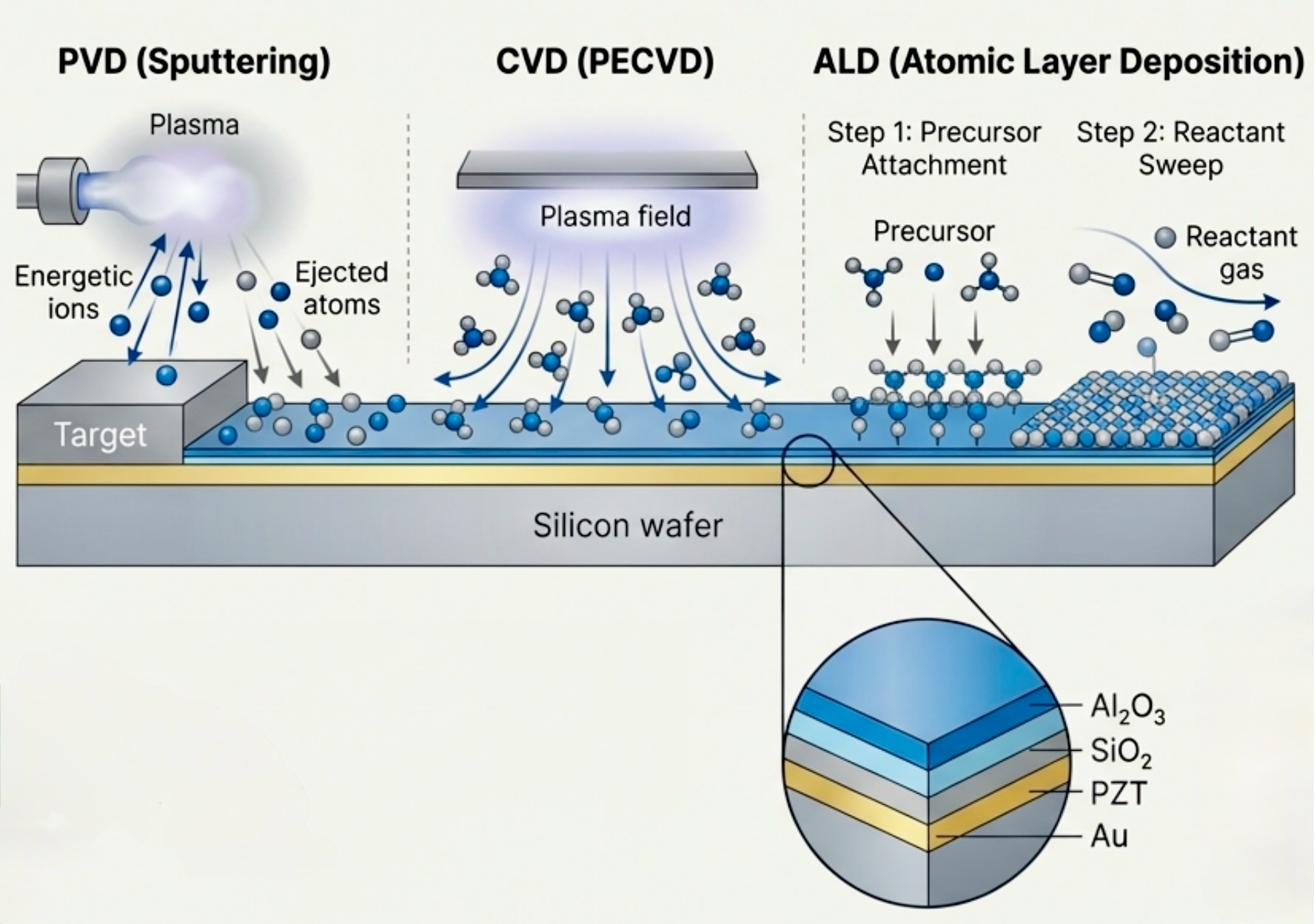
PVD, ALD, MBE,
side by side
Three ways atoms reach a wafer on this line: by line of sight, by self-limiting cycles, and by epitaxy in UHV.
Thin film deposition on
optical-grade fused silica
Fused silica (SiO₂) is a preferred substrate for precision optical coatings and photonic thin film processes. Its broad UV-to-IR transmission window, ultra-low thermal expansion, and chemical stability make it well-suited for deposition processes where substrate outgassing, thermal distortion, or optical interference would compromise film performance.
AR & HR Coatings
Anti-reflection and high-reflection multilayer stacks deposited on fused silica using PVD (e-beam evaporation or ion-beam sputtering). Applied to optical windows, laser output couplers, and photomask blanks where wavelength-specific reflectance control is critical.
Conductive & Functional Films
ITO, metal, and dielectric films on fused silica for electrooptic devices, biosensors, and RF substrates. The low dielectric loss and high chemical purity of optical-grade fused silica minimizes substrate-induced interference in functional film characterization.
TGV Wafer Preparation
Barrier seed layers, metal fill preparation, and dielectric liner films deposited on fused silica wafers prior to or after TGV drilling. We coordinate substrate supply, TGV formation, and thin film steps as a single project engagement.
🟣 Flexible & metallic substrates: PVD thin film deposition is also available on polyimide (PI) film and thin SUS stainless steel - enabling direct deposition of thermocouple alloys, RTD metals, and sensor structures on flexible and metallic substrates.
PI Film & SUS Sensor Fab →Start your project.
Initial response within one business day.
Share your process requirements, substrate, and production volume. A Nanosystems JP Inc. engineer will give an initial response within one business day. Full quote typically within 7-10 business days, subject to project complexity and NDA requirements.