From the airbag accelerometer that is used for crash detection to the SiC inverter that drives the traction motor with 98% efficiency, semiconductor fabrication precision directly determines automotive safety and performance.
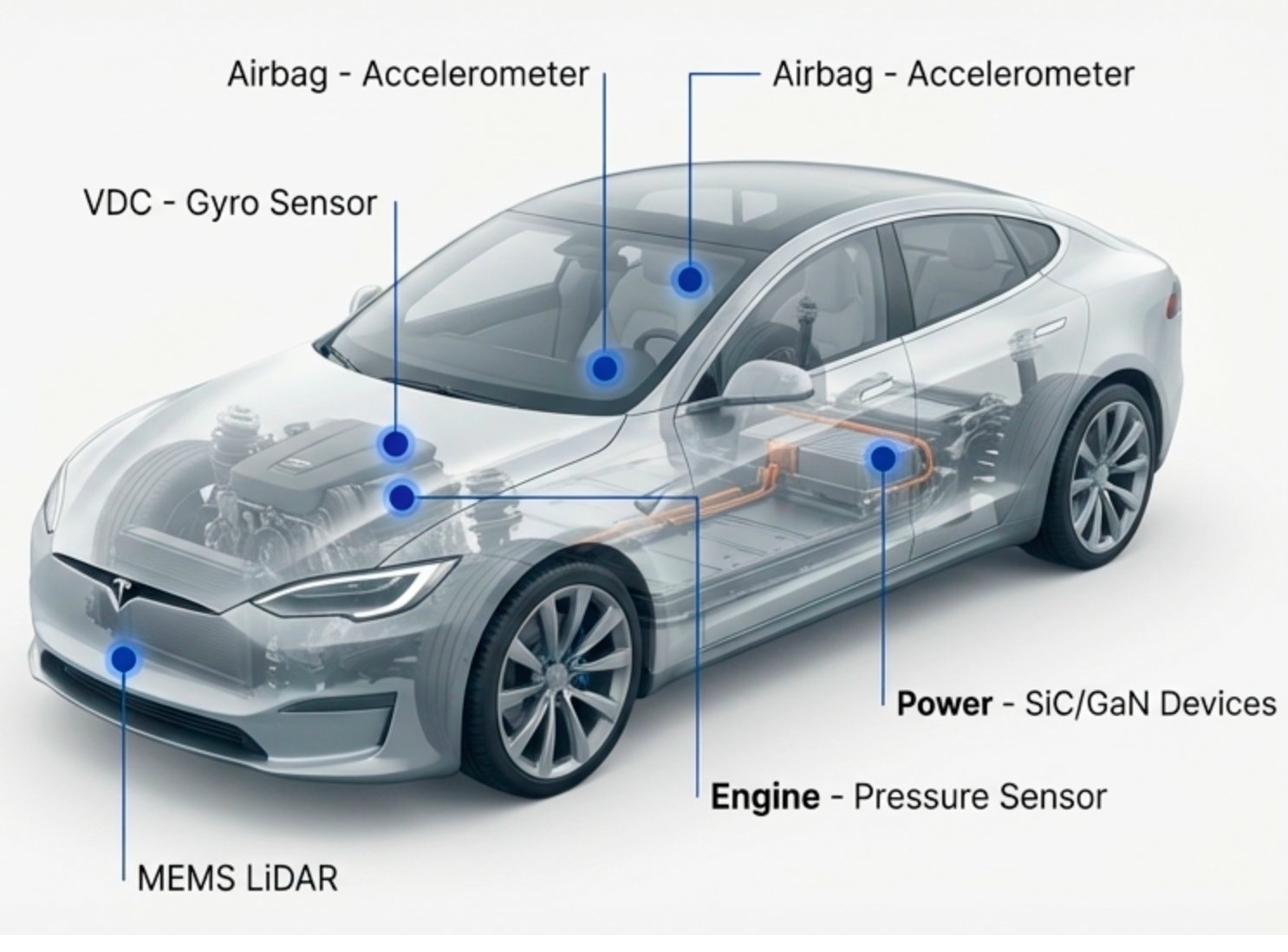
Safety: Airbag & Crash Detection
Airbag systems rely on MEMS accelerometers to detect crash events in under 1 millisecond and trigger inflation. The sensor must reliably detect a 40g impact while surviving normal driving vibration. MEMS fabrication parameters, proof mass geometry, spring stiffness, air damping gap, directly set the g-sensitivity and bandwidth. Our DRIE etching achieves the precise proof mass geometries required for automotive-grade crash sensing.
Stability: VDC & ADAS
Vehicle Dynamic Control (VDC) and advanced driver assistance systems use three-axis accelerometers and three-axis gyroscopes (IMU) to measure vehicle motion 1000 times per second. Drift and offset over temperature are the key reliability challenges, requiring tight process control of MEMS resonator frequency and electrostatic gap. Our ion implantation, DRIE, and wafer bonding services provide the precise device parameters automotive IMUs require.
Perception: MEMS LiDAR
Solid-state MEMS scanning mirrors for automotive LiDAR deflect laser beams across the scene at high speed, replacing bulky rotating mechanical LiDAR units with compact wafer-scale MEMS devices. Mirror flatness, resonant frequency, and scan angle are controlled by MEMS geometry. Our deep DRIE, wafer bonding, and hermetic packaging services create the mirror structures and vacuum cavities essential for high-Q MEMS LiDAR performance.
Powertrain: SiC & GaN Inverters
Electric vehicle traction inverters using SiC MOSFETs switch at 10-100kHz with 98%+ efficiency, enabling smaller cooling systems and longer EV range vs silicon IGBTs. SiC fabrication is demanding: Al and N ion implantation followed by activation annealing at 1400-1800°C in Ar, carbon cap annealing for gate oxide quality, ohmic contact sintering. Our dedicated SiC process flow handles the full device sequence from substrate preparation through metallization.
Environment: Pressure & Gas Sensors
Automotive pressure sensors measure manifold air pressure, tire pressure (TPMS), fuel rail pressure, and exhaust back-pressure. MEMS membrane thickness (controlled by DRIE etch depth) sets the pressure range. Thin membranes for intake manifold (0-100 kPa); thick membranes for fuel rail (0-200 bar). Gas sensors (NOx, CO, O₂) using metal oxide thin films and electrochemical cells for exhaust aftertreatment control.
Comfort: MEMS Microphones
Automotive cabin microphones for voice control, active noise cancellation, and emergency call (eCall) systems use MEMS transducers rather than electret microphones, providing better SNR, smaller size, and better reliability over the automotive temperature range (-40°C to +125°C). MEMS microphone fabrication uses backplate and membrane DRIE with precise air gap control for flat frequency response.
Deep DRIE, Proof Mass & Membrane
DRIE etching with 50:1 aspect ratio creates the proof masses for accelerometers, resonating elements for gyroscopes, and deflecting membranes for pressure sensors. Etch uniformity across the wafer controls matching between adjacent sensor elements, critical for differential measurement systems.
Ion Implantation, SiC Doping
Al (p-type) and N (n-type) ion implantation in 4H-SiC at energies up to 1MeV for MOSFET channel, body, and source region formation. High-temperature activation annealing at 1400-1800°C in Ar. Our SiC-specific implantation and annealing process achieves >80% activation efficiency.
Wafer Bonding, Hermetic MEMS
Anodic bonding and eutectic AuSn bonding create hermetic cavities for MEMS gyroscopes, accelerometers, and LiDAR mirrors. Vacuum-sealed cavities maintain the low-damping environment essential for high-Q MEMS resonators. Glass-Si anodic bonding at 250-450°C for MEMS sensor caps.
Annealing, SiC Gate Oxide
Carbon cap annealing + high-temperature RTA in Ar for SiC surface preparation before gate oxide growth. Surface roughness (RMS) is a key predictor of SiC MOSFET gate oxide reliability and channel mobility. Our carbon cap process achieves the low-RMS surfaces required for automotive-grade SiC.
Dicing, Compound Semiconductors
Diamond scribing of SiC and GaN wafers along crystallographic cleavage planes, avoiding the die-edge micro-cracking that blade dicing causes. Clean die edges are critical for high-voltage blocking capability in SiC MOSFETs. Stealth laser dicing for MEMS devices with fragile membranes.
Packaging, Power Modules
Silver sinter die attach (>200 W/m·K) for SiC/GaN chips in power modules. Heavy Al wire bonding (500µm) for high-current connections. AuSn hermetic sealing for MEMS sensors. Automotive-grade assembly with full lot traceability from wafer to finished module.
SiC and MEMS - managed as one project
SiC power device process flows and MEMS sensor fabrication are managed as one project at Nanosystems JP Inc. When your module integrates sensing and power conversion, you get one point of contact across the full scope.
High-temperature implant anneal to 1800°C
SiC dopant activation at 1400-1800°C in Ar, the most thermally demanding step in automotive power device fabrication, available with carbon cap annealing coordination.
Hermetic MEMS packaging
Anodic bonding and AuSn eutectic for hermetic MEMS sensor cavities meeting automotive reliability requirements. Glass-Si triple-stack bonding for vacuum-sealed gyroscope cavities.
From 1 wafer, fast iteration
Prototype MEMS sensor designs on a single wafer. Iterate proof mass geometry, etch depth, or gap dimension in days rather than waiting for minimum lot commitments.
NDA available on request
Automotive sensor and power device designs are sensitive. An NDA can be arranged before any design files or device parameters are shared, just mention it in your first message. Initial inquiries and quotes can proceed without one.
Start your project.
Initial response within one business day.
Share your process requirements, substrate, and production volume. A Nanosystems JP Inc. engineer will give an initial response within one business day. Full quote typically within 7-10 business days, subject to project complexity and NDA requirements.