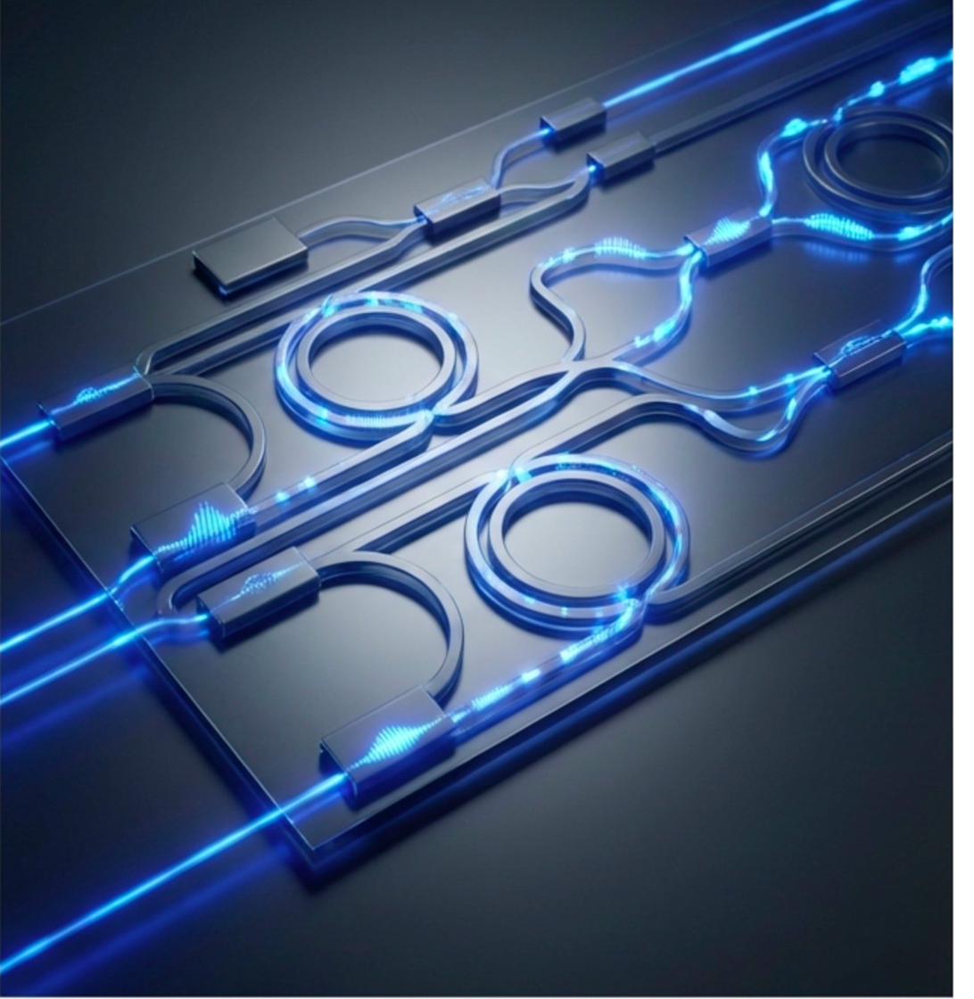
Silicon photonic integrated circuits combine multiple optical functions, waveguiding, modulation, detection, and coupling, on a single Si chip. Fabricating and packaging these devices requires a sequence of precision steps that we provide end-to-end.
SOI Substrate & Waveguide Patterning
Silicon-on-insulator (SOI) wafers provide the high-index Si waveguide core on a buried SiO₂ cladding. KrF stepper patterns the waveguide layer, the most critical lithography step in SiPho fabrication. ICP-RIE etches the Si waveguide to depth while maintaining sidewall smoothness below 2nm RMS. Sidewall roughness directly controls propagation loss, our ICP-RIE targets <2 dB/cm propagation loss at 1550 nm on standard SOI platforms, confirmed per design.
Nanoscale Grating & Coupler Structures
Grating couplers, photonic crystal structures, and sub-wavelength anti-reflection gratings require feature sizes below 100nm, requiring e-beam lithography. E-beam direct-write from GDS file without mask cost, enabling rapid design iteration on sub-100nm SiPho features. For volume production, e-beam master + UV-NIL replication produces sub-wavelength gratings at lower cost. Apodized grating couplers targeting <1 dB fiber-chip coupling loss at 1550 nm (achieved values depend on geometry and fiber mode).
III-V Laser Integration - AuSn Bump Fabrication
Silicon cannot generate light - InP or GaAs laser diodes must be flip-chip bonded onto the SiPho PIC. We fabricate the wafer-level AuSn bumps (80/20 eutectic, PVD multi-layer + lift-off) that make this bonding possible: fluxless, hermetic, with self-aligning surface tension that places the laser facet within ±1µm of the Si waveguide input. Bumped wafers are delivered ready for flip-chip assembly at your facility or chosen assembly site.
TSV & TGV, SiPho Interposer
Silicon or glass interposers with TSV/TGV provide electrical connections between the SiPho PIC, electronic IC (EIC), and package substrate. Our DRIE TSV (50:1 aspect ratio) and TGV (up to 510×510mm glass) enable the vertical signal routing in co-packaged optics modules for 400G/800G/1.6T optical transceivers. Cu damascene RDL routes signals between chiplets at sub-2µm line/space.
Thin Film Deposition Optical Layers
Optical cladding and functional thin films on SiPho devices: PECVD SiO₂ and SiN as upper cladding, ALD Al₂O₃ for passivation, sputtered SiO₂ for planarization before upper cladding deposition. TiO₂ and Ta₂O₅ for high-refractive-index waveguides. epitaxial Ge growth for low-dark-current photodetector regions. PZT piezoelectric thin film for electro-optic modulators. All deposition processes calibrated for optical quality, refractive index and loss are characterized post-deposition. Transparent conductive oxides (ITO, IZO, a-ITO) are also available for electro-optic and sensor integration on glass and flexible substrates.
Stealth Dicing, Clean Waveguide Facets
Standard blade dicing floods the wafer with water at high pressure, water at the waveguide facet causes permanent coupling loss and photoresist contamination of optical surfaces. Stealth laser dicing is the only method that produces clean dry waveguide facets. The laser modifies only the silicon interior; water never contacts the surface. Direct use after dicing, dry, debris-free edges that minimize post-dicing preparation for grating-coupled devices; edge-coupled facets are prepared as required.
Waveguide Combiners & Gratings
AR/VR waveguide display combiners use nanoscale surface gratings to couple light in and out of the waveguide at specific angles. E-beam master + UV-NIL replication produces high-n grating structures at wafer scale. High refractive index NIL resist (n>1.9) enables the strong diffraction efficiency required for compact wearable displays.
Metasurface Flat Optics
Metasurface lenses and beam steerers use sub-wavelength pillar arrays (height 200-800nm, pitch 100-400nm) to control phase, amplitude, and polarization of light. E-beam lithography defines the pillar pattern; ICP-RIE etches into Si, TiO₂, or GaN. Applications: compact camera lenses, LiDAR beam shapers, holographic displays.
MEMS Optical Switches & Mirrors
MEMS-based optical switches for data center optical interconnects and tunable LIDAR use electrostatically actuated Si mirrors and cantilevers. Deep DRIE creates the suspended mirror structures; hermetic wafer bonding seals the mirror in vacuum for high-Q operation. AuSn flip-chip integration with photonic chips in co-packaged modules.
Full SiPho process stack
SOI waveguide patterning, grating e-beam, ICP-RIE etch, thin film cladding, CMP, and TSV, managed end to end by a dedicated project manager across the entire SiPho process.
AuSn laser flip-chip specialist
PVD AuSn bump fabrication and fluxless flip-chip bonding of InP/GaAs laser sources onto SiPho PICs, with ±1µm self-aligning accuracy. AuSn bumped wafers ready for co-packaged optics assembly.
Stealth dicing preserves facets
Dry stealth laser dicing is the only dicing method that preserves optical waveguide facets. Standard blade dicing permanently degrades coupling efficiency, we use stealth as default for all SiPho wafers.
TSV + TGV interposer both available
Silicon (TSV) and glass (TGV to 510×510mm) interposers, both. Glass provides lower dielectric loss for RF signals at 100+ GHz alongside optical routing in SiPho modules.
NIL for high-volume photonics
E-beam master + UV-NIL replication for high-volume production of waveguide gratings, metasurface lenses, and diffraction elements at lower cost than repeated e-beam exposure.
NDA available on request
Photonic device designs are sensitive. An NDA can be arranged before any GDS files or process specifications are shared, just mention it in your first message. Initial inquiries and quotes can proceed without one.
Start your project.
Initial response within one business day.
Share your process requirements, substrate, and production volume. A Nanosystems JP Inc. engineer will give an initial response within one business day. Full quote typically within 7-10 business days, subject to project complexity and NDA requirements.