The biomedical device market spans three scales: nano (DNA, protein, single molecule), micro (cell, organoid, tissue), and device (implant, diagnostic instrument). Our fabrication capabilities address all three.
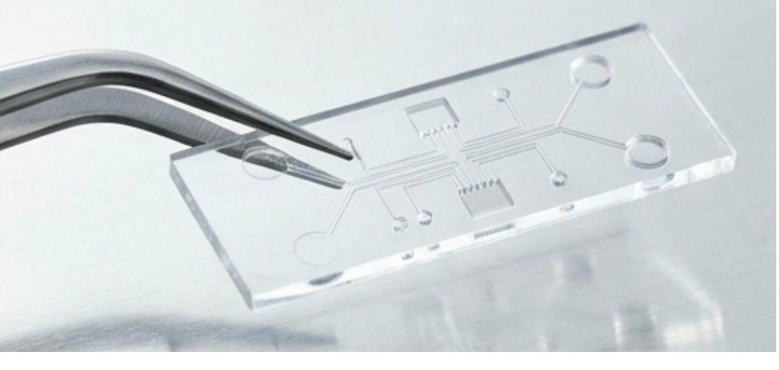
Organ-on-Chip (OoC)
Multilayer PDMS chips with pneumatic Quake valves, peristaltic pumps, and thin flexible membranes replicate the microenvironment of human organs, lung, gut, kidney, brain, liver, and heart, for drug discovery and toxicity testing. PDMS soft lithography from SU-8 masters enables 3-5 day design-to-chip turnaround. COP injection-molded versions for production volumes where PDMS autofluorescence is a concern.
Micro-Electrode Arrays (MEA)
Planar and 3D MEA for extracellular neural signal recording, stimulation, and drug response monitoring. Pt or TiN electrode arrays on glass or Si substrate patterned by lift-off. SU-8 or polyimide passivation with electrode openings at recording sites. DRIE through-holes for 3D probe insertion. Biocompatible PI RDL for flexible implantable probe variants.
DNA Sequencing Flow Cells
Glass flow cells with NIL-defined nanopore arrays (<50nm) for nanopore sequencing, or precision microchannels for optical sequencing. Fusion or anodic bonding for hermetic glass-glass or glass-Si seals with no adhesive in the optical path. Large-format glass processing (500×600mm) enables 96-well or 384-well array formats at low cost-per-chip, critical for sequencing instrument economics.
LSPR Biosensors
Localized surface plasmon resonance chips with gold nanopillar or nanohole arrays on glass, fabricated by NIL and Au lift-off. The nanostructured gold surface is functionalized with antibodies, aptamers, or nucleic acid probes for label-free detection of cancer biomarkers, pathogen proteins, and nucleic acids. Sensitivity 10-100× higher than flat Au SPR chips due to localized field enhancement.
Drug Delivery Microdevices
Ni and Pd-Ni microneedle arrays by LIGA electroforming for transdermal drug delivery and interstitial fluid (ISF) sampling. Hollow microneedles with 1µm-diameter fluid channels. Droplet microfluidic chips for monodisperse microencapsulation of drug-loaded particles (CV <2%). Pd-Ni biocompatible grade for implant-contact applications.
Implantable Neural Interfaces
Neural probes and implantable sensors using biocompatible PI RDL and Au/Pt electrodes. Hermetic AuSn sealing for implantable optical transceivers (retinal implants, deep brain stimulators). Polyimide selected and evaluated for the intended medical-device application for electrode passivation. NDA-protected, your implant design remains confidential from first technical discussion.
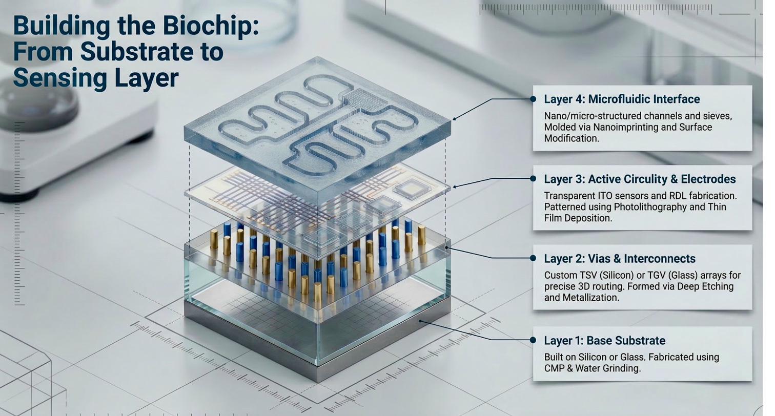
PDMS Soft Lithography
SU-8 master on Si wafer → PDMS cast and cure → O₂ plasma bond to glass or PDMS. The fastest route from biochip design to working prototype. 3-5 days from GDS to first functional chip. Multilayer for Quake valves and 3D channel networks.
NIL Nanopores & LSPR
E-beam master + UV/thermal NIL for sub-50nm nanopores and Au nanostructure arrays. All: master fabrication, NIL, dry etch transfer, and Au lift-off on the same substrate.
Thin Film Deposition Bioelectrodes
Au, Pt, ITO, and TiN electrode deposition by PVD sputtering and evaporation. Lift-off patterning for electrode arrays with sub-5µm features. ITO for transparent electrodes in optogenetics and fluorescence biochips.
Glass Bonding
Anodic bonding (glass-Si, hermetic) and fusion bonding (glass-glass, UV-transparent) for biochip sealing. C-SAM inspection on every bond. Large-format to 500×600mm.
Injection Molding (COP/PC)
PC and COP chip production via injection molding, from SU-8/PDMS prototype to mass-produced polymer chip. Mold tooling fabricated. COP for low autofluorescence fluorescence assays.
LIGA Microneedles
Ni and Pd-Ni microneedle arrays by X-ray LIGA electroforming. 1µm hollow channel diameter. Biocompatible Pd-Ni for ISF sampling and drug delivery applications.
500×600mm glass for low chip cost
Panel-scale glass biochip processing produces 5-10× more chips per run versus wafer-format foundries, dramatically reducing cost-per-chip for array biosensors and diagnostic plates.
PDMS prototype in 3-5 days
From SU-8 master fabrication to first functional PDMS chip in 3-5 days. Iterate channel geometry, valve placement, or electrode layout rapidly without waiting for minimum lot commitments.
Sub-50nm nanopores
NIL nanopore arrays for DNA sequencing, nanofluidic confinement, and molecular sieving, with master mold fabrication and pattern transfer done. Nanofabrication is included in the same project.
Biocompatible materials, PI and Pd-Ni
Polyimide selected and evaluated for the intended medical-device application for electrode passivation in implantable devices. Pd-Ni electroforming for biocompatible microneedles and microstructures in direct contact with biological tissue.
PDMS to production, same design
Prototype in PDMS, then transition to injection-molded COP with the same channel design. Mold tooling. No redesign for a different foundry process.
NDA available on request
Biomedical device designs, assay protocols, and surface chemistry specifications are among the most sensitive in any industry. An NDA can be arranged before any design files or technical details are shared, just mention it in your first message. Initial inquiries and quotes can proceed without one.
Start your project.
Initial response within one business day.
Share your process requirements, substrate, and production volume. A Nanosystems JP Inc. engineer will give an initial response within one business day. Full quote typically within 7-10 business days, subject to project complexity and NDA requirements.