Pure-play foundry
from Japan
At Nanosystems JP Inc., we specialize in pure-play foundry services for semiconductor, MEMS and nanofabrication projects, from substrate procurement to diced chips, delivered worldwide.
Supporting engineers, R&D teams, and technical organizations
We work with engineers, R&D teams, startups, and manufacturing organizations that need dependable fabrication support without building internal process infrastructure. Our role is to translate process requirements into wafer-level execution, from early prototyping through production-scale builds.
Japanese precision
Cleanroom fabrication executed to Japanese quality standards, with the precision and attention to detail Japan is known for globally.
End-to-end
Substrate sourcing, mask preparation, process execution, dicing, and delivery can be managed within one program.
Accessible
Small-lot prototyping from 1-5 wafers with no prohibitive minimums. From R&D to production scale without changing foundries.
IP protection
NDA available before you share any design details. Your technology stays protected from first contact to final delivery.
Technical foundry
Engineer-led communication, project discussions handled with technical input from the beginning.
Global reach
Global logistics and English-language technical support for international R&D teams.
One project manager, one quotation, one point of contact
Every program at Nanosystems JP Inc. is managed end to end by a dedicated project manager. You receive one quotation, one process traveler, and one point of contact from feasibility review through delivery. Engineering questions are answered by process engineers, not a sales desk. Confidential designs are handled under NDA on request. Milestone reports follow the traveler, from lithography through dicing, and every delivery ships with its inspection data.
Marunouchi, Chiyoda-ku, Tokyo
English and Japanese
Based in central Tokyo
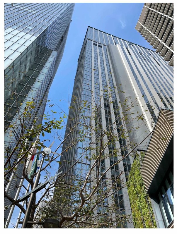
Nanosystems JP Inc. is headquartered at Marunouchi Trust Tower Main Building, in the heart of Tokyo's business district, close to Tokyo Station.
Nanosystems JP Inc.
株式会社ナノシステムズJP
Marunouchi Trust Tower Main Building, 20F
1-8-3 Marunouchi, Chiyoda-ku
Tokyo 100-0005, Japan
✉ sales@nanosystemsjp.co.jp
📞 +81-3-5288-5569
🌐 www.nanosystemsjp.co.jp
20+ processes across the full semiconductor fabrication flow
At Nanosystems JP Inc., we offer a complete range of front-end and back-end semiconductor processes, from bare substrate to fully packaged chip.
Front-End Processes
Substrate procurement, mask fabrication, lithography (e-beam 20 nm to panel-scale steppers), nanoimprinting, thin film deposition (100+ materials), electroplating, etching, annealing, ion implantation, CMP, and dicing.
3D IC & Interposers
TSV fabrication, TSV reveal, TGV fabrication, wafer bonding (eight methods), RDL fabrication, UBM, C4 bumping, AuSn bump services for silicon photonics, and full packaging assembly.
Biochip & Photonics
Glass/silicon/polymer biochip fabrication, organ-on-chip, MEA devices, silicon photonics waveguide processing, LIGA electroforming, and roll-to-roll thin film deposition.
Get in touch with our team
At Nanosystems JP Inc., a process engineer will review your inquiry personally. We give an initial response typically within one business day, with a full quote typically within 7-10 business days, subject to project complexity and NDA requirements.
Process requirements, substrate type and size, production volume, and your target timeline. GDS/DXF files are not required at this stage.
An NDA can be arranged before any design files or technical details are shared, just mention it in your first message.
Initial response typically within one business day. Full quote typically within 7-10 business days once all project information is confirmed.