TGV Fabrication
At Nanosystems JP Inc., we offer Through-Glass Via microfabrication for 2.5D/3D packaging, RF MEMS, photonics, and biomedical devices. Precision diameters from 20µm, panels to 510×510mm, and repeatable fill quality.
(typical)
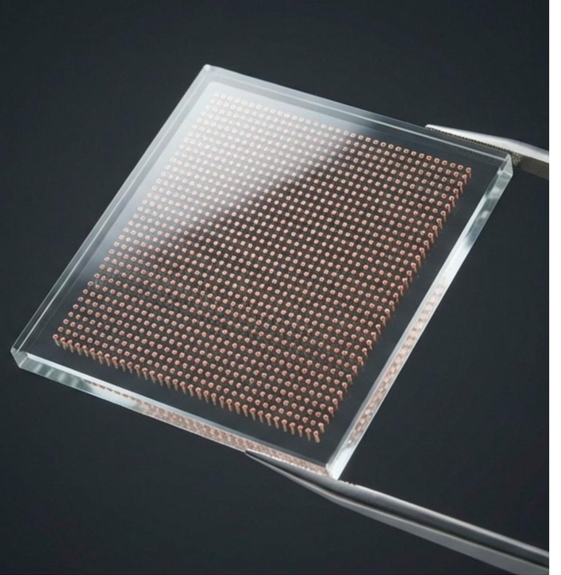
Glass interposers for cost-effective
2.5D & 3D packaging
TGVs play an important role in advanced wafer packaging. Glass offers distinct advantages over silicon, especially for RF applications, optical devices, and scenarios where CTE matching with organic substrates is critical.
Precision Via Dimensions
Tight control over via geometry, diameter, shape, and depth all customizable to your design requirements.
Via Shapes
Three through-via shapes plus blind vias (BGV). Via shape is selected based on diameter requirements and application, each offering different filling characteristics and mechanical properties.
Substrate Size Flexibility
From standard wafer formats to large-panel production, one foundry for prototyping and volume.
Diverse Glass Types
Four glass types plus sapphire, covering RF, optical, display, and high-durability applications, each with distinct electrical and thermal properties.
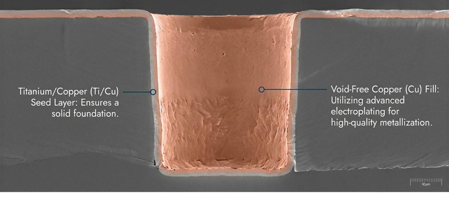
High-Quality Cu Fill
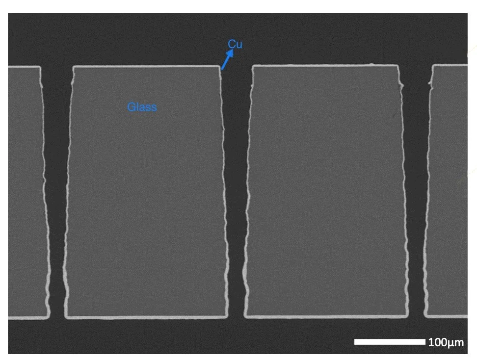
Ti/Cu seed layer + Cu electroplating for conformal or void-free fill. Low resistance. Fill quality verified by SEM cross-section.
Complete Post-Processing
Beyond via formation, full substrate finishing services coordinated in the same project flow.
After via formation, copper metallization is applied using an advanced Ti/Cu seed layer followed by electroplating. Two fill modes are available depending on your electrical and structural requirements. Completely filled vias offer lower resistance and direct thermal conduction. Conformal vias coat the sidewalls while leaving a hollow core - suited for RF shielding structures and applications where fill is not required.
High aspect ratio hollow vias: When copper fill is not required, glass TGV holes alone can achieve aspect ratios of 20:1 as a standard target, with higher ratios available on request. The Cu fill constraint is the limiting factor for high-AR vias - the via geometry itself is not. This makes hollow high-AR TGV practical for optical through-apertures, fluid channels, vent holes in hermetic packages, and coaxial RF via structures where only a conformal sidewall coating is needed.
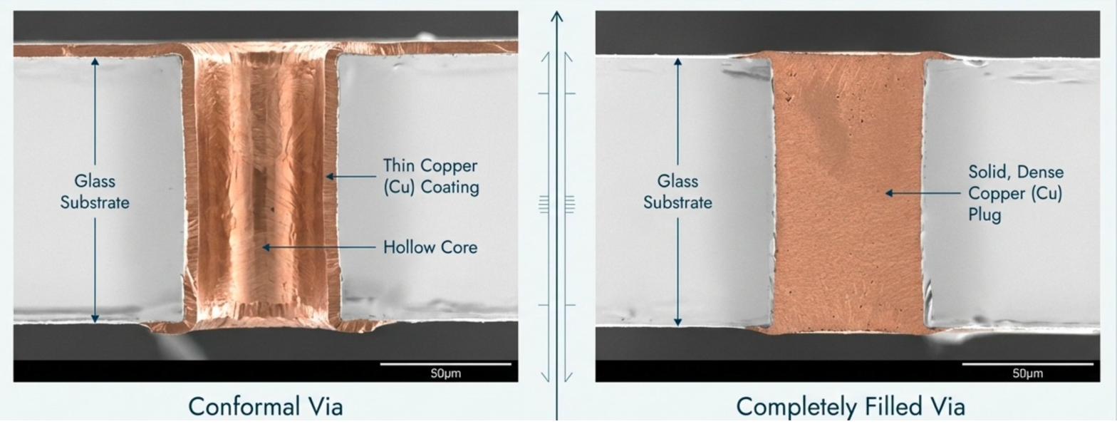
Thin Cu coating on via sidewalls and base - hollow core remains. Faster plating cycle, lower Cu consumption. Suitable where conductivity rather than void-free fill is the priority: RF shielding coaxial vias, signal routing where resistance spec allows hollow geometry.
Solid dense Cu plug filling the entire via volume, void-free verified by SEM cross-section. Lowest electrical resistance and highest thermal conductivity. Required for 3D-IC interposers, power delivery vias, and any application where via yield reliability and signal integrity are critical.
Complete TGV process parameters
All parameters can be customized for your specific application. Contact our engineers to discuss requirements outside the ranges listed.
| Parameter | Specification | Notes |
|---|---|---|
| Min via diameter | 20µm | Smaller possible on request |
| Via diameter variation | Multiple diameters on same substrate | Different diameters front/back possible (e.g. 30µm / 60µm) |
| Via shapes | Hourglass, Straight, Tapered | Shape depends on diameter and application |
| Aspect ratio | Up to 10:1 (depth:diameter) | Higher AR on request for select glass types |
| Substrate sizes | 100mm, 200mm, 300mm wafers; up to ~510×510mm panels | Non-standard sizes available |
| Ultra-thin substrate | Down to 50µm | Requires carrier handling |
| Blind Glass Vias (BGV) | Available | Single-side via for partial depth interconnect |
| Glass types | Borosilicate, Soda lime, Fused silica, Sapphire, Alkali-free | See glass comparison below |
| Cu fill type | Void-free fill or conformal coating | Void-free recommended for low resistance |
| Seed layer | Ti/Cu by sputtering | Ensures adhesion and plating uniformity |
| Fill verification | SEM cross-section | Every lot, post-fill before CMP |
| Cu CMP | Available | Planarizes surface for RDL or bonding |
| Optical polishing | Optical-level CMP | For photonic and optical applications |
| RDL | Double-sided RDL on TGV substrate | Polymer passivation or Cu damascene |
| Anodic bonding | Available | Glass-to-silicon wafer bonding service |
| Thin film metallization | Available | Sputtering, e-beam evaporation, ALD |
Use these rules when designing your TGV interposer layout. Parameters outside these ranges are possible on inquiry - contact our engineers with your specific requirements before taping out.
| Parameter | Min | Typical | Max / Notes |
|---|---|---|---|
| Via diameter | 20µm | 50-100µm | Smaller on request; larger → lower aspect ratio |
| Via pitch | 2× via diameter | 150-300µm | Min spacing = 1× via diameter (wall-to-wall) |
| Via wall-to-wall spacing | 1× via diameter | 50-200µm | Tighter possible with straight-wall vias |
| Via-to-edge clearance | 200µm | 500µm | From via center to substrate edge |
| Via-to-via diameter mismatch | - | - | Multiple diameters on same substrate OK; front/back differ e.g. 30µm / 60µm |
| Aspect ratio (depth ÷ diameter) | 1:1 | 5:1 | Up to 10:1 (Cu-filled). Hollow / unfilled vias: 20:1 typical, higher on request; the Cu fill, not the hole, sets the limit for filled vias |
| Glass substrate thickness | 50µm | 300-500µm | Thinner requires temporary carrier bonding |
| Cu land pad diameter | Via ø + 20µm | Via ø + 50µm | Applies on both sides for void-free fill |
| RDL line width / space | 10µm / 10µm | 20µm / 20µm | Polymer passivation or Cu damascene |
| RDL to via pad keepout | 10µm | 20µm | From RDL edge to land pad edge |
| Solder bump pitch (on TGV RDL) | 100µm | 150-300µm | C4 SnAg or AuSn bumping available after RDL |
| Panel dicing street width | 100µm | 200µm | For panel format (up to 510×510mm) |
standard
fill on request
select glass only
- Submit GDS or DXF - our engineers review design rules before processing
- Specify glass type and target thickness early - affects via shape options
- Confirm fill type (void-free vs conformal) before layout finalization
- BGV (Blind Glass Via) requires minimum 2× diameter depth margin
- RDL layers can be added both sides after Cu CMP
Via shape is determined by the formation method and glass type. Hourglass and straight are the most common; tapered suits certain deposition requirements; Blind Glass Vias (BGV) penetrate only partway through the substrate for single-sided interconnects, depth sensors, and optical windows.
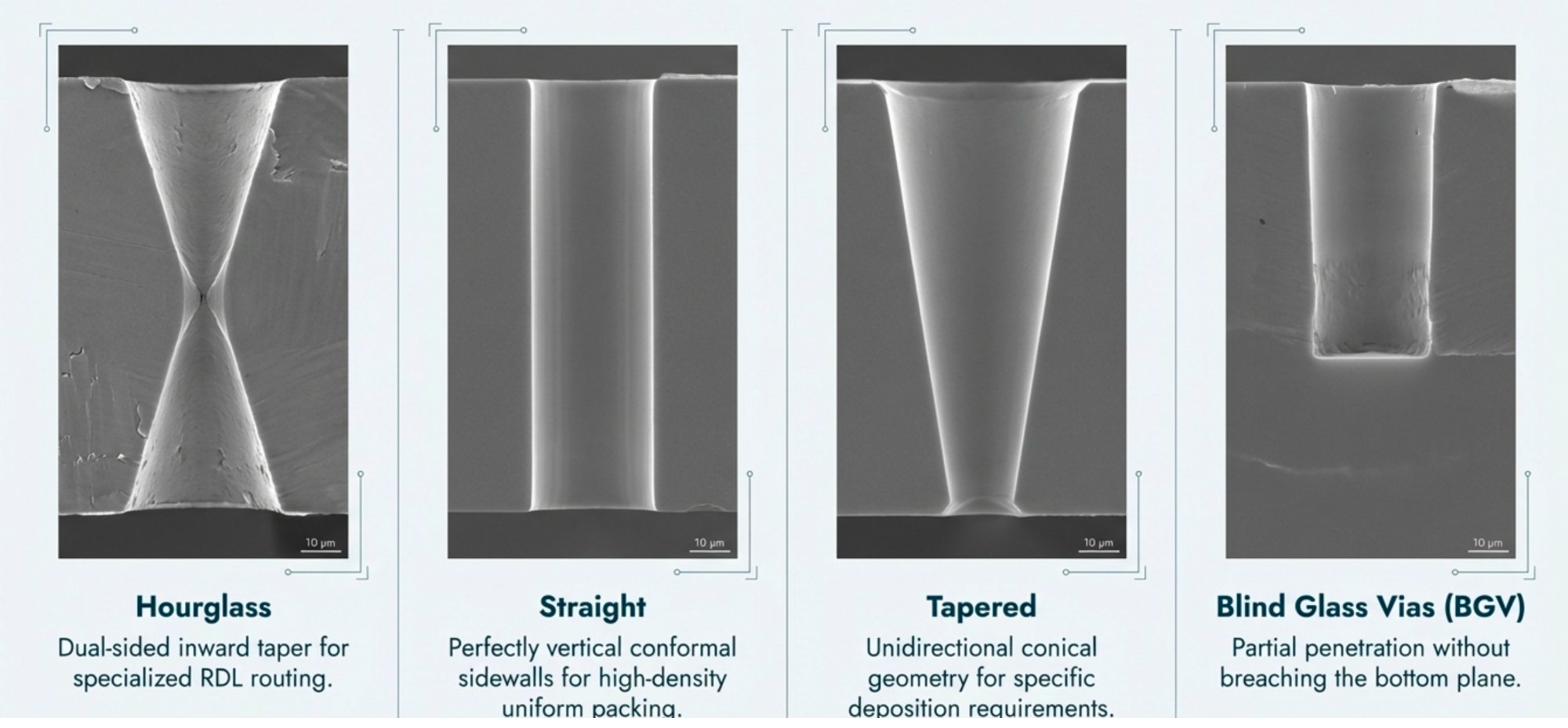
Dual-sided inward taper formed by laser drilling from both sides. Ideal for RDL routing where slight taper aids conformal metal coverage. Most common shape for standard TGV interposers.
Perfectly vertical sidewalls for maximum packing density and tightest via pitch. Requires precise laser parameter control. Best choice for high-density interconnect arrays.
Unidirectional conical profile, wider at entry, narrower at exit. Provides easier metal seed layer coverage and more reliable conformal or void-free Cu fill for larger diameter vias.
Partial penetration - via is drilled only partway through the glass substrate without breaching the bottom plane. Used for single-sided interconnects, optical windows, depth sensors, and capacitive structures requiring a closed bottom.
Five substrate types, matched to your application
Each glass type brings distinct electrical, optical, thermal, and mechanical properties. We can advise on the best choice for your specific application.
Borosilicate Glass
High resistivity. Low electrical loss. Adjustable CTE, better match with organic substrates than silicon. Low-loss tangent for RF.
Soda Lime Glass
Cost-effective for large-panel production. Standard display glass composition. Available in the largest panel formats.
Fused Silica (synthetic quartz glass)
UV to IR optical transparency. Minimal electrical loss. Highest thermal stability. Ideal for photonic and optical interposers.
Sapphire
Extreme hardness (Mohs 9). High thermal conductivity. Chemical resistance. For demanding environments requiring robustness.
Alkali-Free Glass
Very low alkali content. Minimized ion migration. Improved electrical properties for high-frequency and precision applications.
| Property | Glass (TGV) | Silicon (TSV) |
|---|---|---|
| Electrical resistance | Very high (insulator) | Semiconductor (variable) |
| RF / HF loss | Very low (low-loss tangent) | Higher substrate loss |
| CTE match (organic PCB) | Better match (adjustable) | Larger mismatch |
| Optical transparency | Yes (visible to UV/IR) | Opaque (visible light) |
| Large panel format | Yes (up to 510×510mm) | Limited to wafer sizes |
| Cost (large volume) | Lower (panel format) | Higher per unit area |
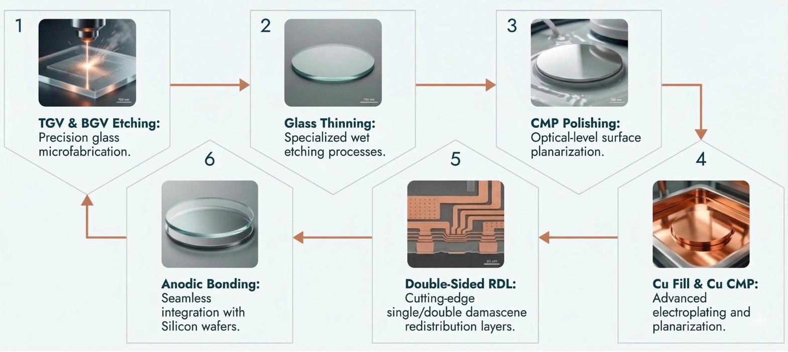
From bare glass substrate to Cu-filled, planarized vias ready for RDL and bumping, all steps managed as one project.
Via Formation
Vias are formed in the glass substrate using laser ablation or sandblasting, creating the precise diameter and shape profile required. Diameter, shape, and pitch are defined at this stage.
Glass Cleaning & Surface Preparation
Via sidewalls and substrate surfaces are cleaned and conditioned to ensure excellent adhesion of the subsequent seed layer. Surface roughness is controlled for optimal plating.
Ti/Cu Seed Layer Deposition
Titanium adhesion layer followed by copper seed layer deposited by sputtering. Conformal coverage into via sidewalls is critical for uniform electroplating. High step coverage achieved.
Cu Electroplating, Void-Free Fill
Copper electroplating fills the vias completely (void-free) or conformally. Optimized plating chemistry and parameters ensure consistent fill quality and repeatable fill quality.
Cu CMP Planarization
Chemical mechanical polishing removes excess copper from the substrate surface, creating a flat, smooth surface with exposed via tops. Optical-level polishing available for photonic applications.
RDL, Metallization & Bonding
Post-CMP processing: Redistribution Layer (RDL) fabrication on one or both sides routes electrical connections. Thin film metallization, anodic bonding with silicon, and further packaging steps available.
Void-free fill &
conformal via options
Two Cu fill methods are available depending on your via diameter, aspect ratio, and electrical requirements. Both use Ti/Cu seed + electroplating.
Complete Cu fill from bottom up. Lowest resistance. Best for high-current and signal integrity applications.
Cu coats via sidewalls and bottom. Lower Cu volume. Suitable for RF shielding and impedance-controlled via structures.
We offer RDL fabrication on both sides of TGV glass substrates, enabling dense fan-out routing for advanced packaging. Two process routes available:
TGV technology across industries
From advanced semiconductor packaging to biomedical lab-on-chip, TGV glass substrates serve a uniquely broad range of high-performance applications.
2.5D & 3D IC Integration
Glass interposer chips for cost-effective 2.5D and 3D wafer packaging. Lower cost per unit area than silicon interposers in large panel format.
RF Devices & RF MEMS
Low-loss RF substrates for mmWave and 5G. RF MEMS switches, resonators, and filters on high-resistivity glass with minimal substrate loss.
High-Performance Computing
High-density glass interposers for AI accelerators, HPC memory stacking, and chiplet integration with tight pitch via arrays.
Optoelectronics & Photonics
Optical transparency enables photonic integration. TGV glass interposers for silicon photonics packaging and wafer-level optics.
Display Panels
Large panel TGV for display driver interconnects. Enables finer pixel pitch and reduced bezel in next-generation flat panel displays.
Biomedical & Cell Culture
BGV (Blind Glass Via) arrays for single-cell experiments. Microfluidic glass chips with integrated TGV electrical connections.
Lab-on-Chip & Microfluidics
Glass microfluidic chips with TGV electrical feedthroughs, combining microfluidics with integrated sensing and actuation electronics.
Shadow Masks & LED
Glass shadow masks as an alternative to metal masks for deposition patterning. TGV glass substrates for LED thermal management.
MEMS Packaging
Hermetic glass-silicon MEMS packaging using anodic bonding. TGV provides electrical feedthroughs through the glass cap layer without breaking the seal - a core requirement for vacuum-packaged resonators and inertial sensors.
Wafer-Level Optics
Fused silica TGV substrates for wafer-level lens arrays, optical sensors, and miniaturized camera modules requiring UV transparency.
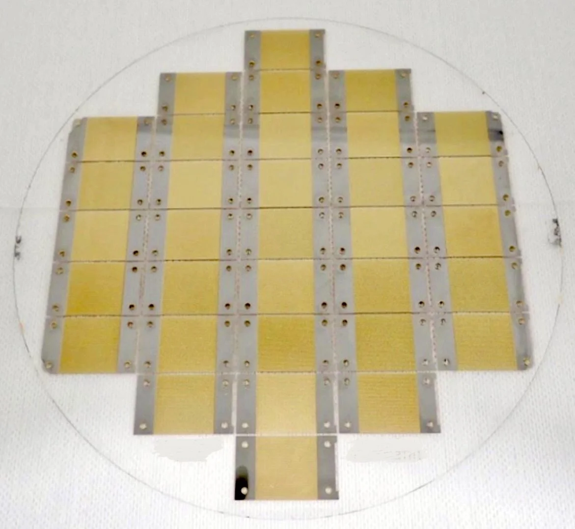
Sample images from TGV programs delivered by Nanosystems JP Inc.
Fused silica TGV for
hermetic device enclosures
When a device package requires both electrical signal routing and a hermetically sealed cavity - such as a vacuum-packaged MEMS resonator or an optoelectronic module - TGV in fused silica provides the feedthrough path through the glass cap layer without compromising seal integrity. The approach combines TGV formation in a fused silica wafer with a subsequent wafer-level bonding step, creating a sealed enclosure with embedded via connections.
Glass cap with through-via feedthroughs
A borosilicate or fused silica glass wafer is drilled with TGV, filled with copper, and then bonded onto the device wafer as the package cap (anodic bonding for borosilicate; intermediate-layer or adhesive bonding for fused silica). Electrical signals pass through the glass without any gap in the hermetic boundary - the via metal is co-sealed during bonding.
Optical transparency through the cap
Fused silica's broad UV-to-IR transmission makes it suitable for optical sensor packages where light must pass through the cap layer - LIDAR windows, IR detector covers, and wafer-level camera modules - while TGV provides the electrical connections on the same substrate.
Low-outgassing cap material
For MEMS devices requiring a stable vacuum or inert-atmosphere cavity, fused silica offers low gas permeability and minimal outgassing compared to polymer-based or metal cap materials. Combined with a hermetic wafer-level bond, it maintains cavity conditions over the device operating life.
Process coordination note: We supply the fused silica wafer, form the TGV, and coordinate the bonding step as a single project. If your design requires RDL or metal redistribution on the glass cap as well, that can be included in the same process flow. Contact us with your cap layer drawing and we will confirm the full process sequence.
Hole-only, seeded, lined, or filled coupons for process evaluation before a full build.
Start your project.
Initial response within one business day.
Share your process requirements, substrate, and production volume. A Nanosystems JP Inc. engineer will give an initial response within one business day. Full quote typically within 7-10 business days, subject to project complexity and NDA requirements.