From the airbag accelerometer that deploys in 1ms to the SiC inverter that drives the traction motor with 98% efficiency, semiconductor fabrication precision directly determines automotive safety and performance.
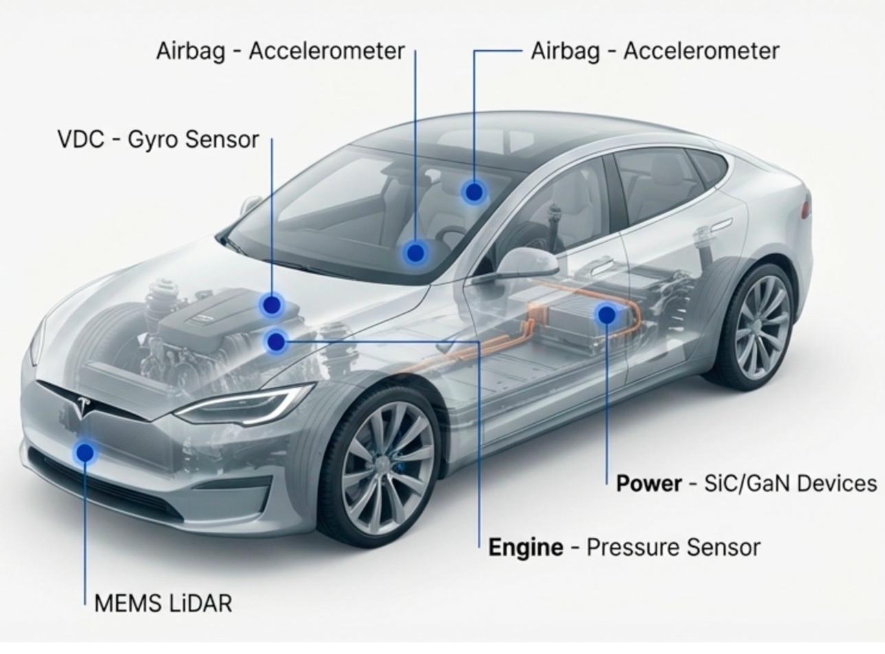
Safety: Airbag & Crash Detection
Airbag systems rely on MEMS accelerometers to detect crash events in under 1 millisecond and trigger inflation. The sensor must reliably detect a 40g impact while surviving normal driving vibration. MEMS fabrication parameters, proof mass geometry, spring stiffness, air damping gap, directly set the g-sensitivity and bandwidth. Our DRIE etching achieves the precise proof mass geometries required for automotive-grade crash sensing.
Stability: VDC & ADAS
Vehicle Dynamic Control (VDC) and advanced driver assistance systems use three-axis accelerometers and three-axis gyroscopes (IMU) to measure vehicle motion 1000 times per second. Drift and offset over temperature are the key reliability challenges, requiring tight process control of MEMS resonator frequency and electrostatic gap. Our ion implantation, DRIE, and wafer bonding services provide the precise device parameters automotive IMUs require.
Perception: MEMS LiDAR
Solid-state MEMS scanning mirrors for automotive LiDAR deflect laser beams across the scene at high speed, replacing bulky rotating mechanical LiDAR units with compact wafer-scale MEMS devices. Mirror flatness, resonant frequency, and scan angle are controlled by MEMS geometry. Our deep DRIE, wafer bonding, and hermetic packaging services create the mirror structures and vacuum cavities essential for high-Q MEMS LiDAR performance.
Powertrain: SiC & GaN Inverters
Electric vehicle traction inverters using SiC MOSFETs switch at 10-100kHz with 98%+ efficiency, enabling smaller cooling systems and longer EV range vs silicon IGBTs. SiC fabrication is demanding: Al and N ion implantation at 1400-1800°C in Ar, carbon cap annealing for gate oxide quality, ohmic contact sintering. Our dedicated SiC process flow handles the full device sequence from substrate preparation through metallisation.
Environment: Pressure & Gas Sensors
Automotive pressure sensors measure manifold air pressure, tire pressure (TPMS), fuel rail pressure, and exhaust back-pressure. MEMS membrane thickness (controlled by DRIE etch depth) sets the pressure range. Thin membranes for intake manifold (0-100 kPa); thick membranes for fuel rail (0-200 bar). Gas sensors (NOx, CO, O₂) using metal oxide thin films and electrochemical cells for exhaust aftertreatment control.
Comfort: MEMS Microphones
Automotive cabin microphones for voice control, active noise cancellation, and emergency call (eCall) systems use MEMS transducers rather than electret microphones, providing better SNR, smaller size, and better reliability over the automotive temperature range (-40°C to +125°C). MEMS microphone fabrication uses backplate and membrane DRIE with precise air gap control for flat frequency response.