Packaging for
3D/2.5D IC Integration
At Nanosystems JP Inc. we offer the complete 3D and 2.5D IC packaging stack. TSV (DRIE etch to 50:1; Cu-filled vias to ~10:1), TGV glass interposer to 510 × 510 mm, TSV/TGV reveal, redistribution layer (RDL), polyimide film interposer, UBM, and C4 bumping. For HBM stacking, chiplet integration, MEMS-on-CMOS, and silicon photonics co-packaging. Every step, one project.
panel size
aspect ratio
end to end
Stacking dies vertically and tiling
chiplets side-by-side
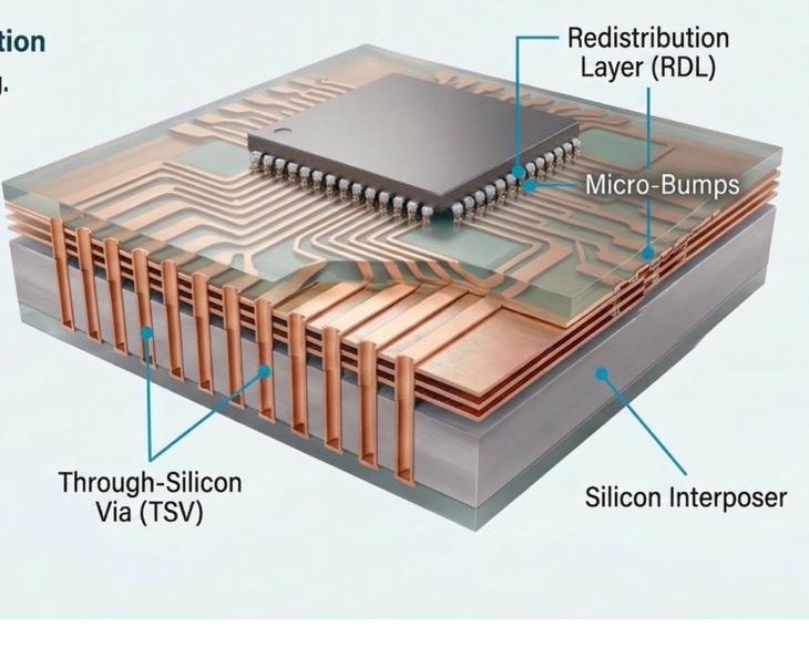
3D-IC stacks dies vertically connected by TSV, achieving the highest bandwidth density (HBM) and shortest inter-die distance. 2.5D places chiplets side-by-side on a common interposer, enabling heterogeneous integration of dies from different foundries and nodes. Both approaches are available at Nanosystems JP Inc.
3D-IC, Vertical Stacking
Dies stacked face-to-face or face-to-back and connected by TSV arrays, the architecture of High-Bandwidth Memory (HBM). TSV provides vertical electrical connections with sub-10 µm pitch, enabling far higher bandwidth density than package-level wire bonding or flip-chip on organic substrate. Each die in the stack requires TSV fabrication, reveal, and micro-bump formation before stacking.
2.5D, Chiplet Integration on Interposer
Multiple chiplets (CPU, HBM, I/O, analog) placed side-by-side on a silicon or glass interposer. The interposer provides high-density RDL routing between chiplets at finer pitch than an organic package substrate can achieve. TSV or TGV in the interposer connects front-side chiplets to back-side C4 bumps for bonding to the organic package substrate. Enables heterogeneous integration of dies from different foundries.
Why a Single-Point Integration Flow Matters
A typical 3D/2.5D integration process involves many sequential steps, each with its own quotation, schedule, and hand-off. Managing them separately increases the risk of specification drift, handling damage (especially for thin wafers), and schedule delays. A delay at any one step can cascade and impact the entire project timeline.
At Nanosystems JP Inc. we provide a single-point integration approach, managing the full process flow from start to finish. All steps are coordinated under a unified framework, ensuring consistency and continuity throughout the project.
- All steps planned and scheduled as one project
- Consistent process management across all steps
- Continuous data tracking with no information gaps
- One schedule, one project
This approach ensures higher reliability, better communication, and smooth execution, especially for complex prototyping projects.
From blank silicon or glass
to bumped, assembly-ready interposer
Each step builds directly on the previous, and the quality of each step determines the yield of all subsequent steps.
TSV Fabrication
Through-Silicon Via fabrication using DRIE Bosch process: 50:1 aspect ratio, over 100 µm depth. Five sub-steps: SiO₂ hard mask DRIE etch, PECVD SiO₂ or ALD Al₂O₃ dielectric liner, TiN/Ta barrier and Cu seed sputtering, Cu electroplating for full fill with superfill additive chemistry, and CMP endpoint-controlled planarization. All five steps, sequenced without inter-step wafer exposure. Full fill verified by cross-section SEM before CMP. Via-first, via-middle, or via-last timing supported depending on device architecture and thermal budget.
TGV Fabrication (Glass Interposer Option)
For applications requiring lower dielectric loss than silicon, RF front-end modules, optical interposers, glass interposers with Through-Glass Vias (TGV) provide a superior substrate. Our TGV capability supports borosilicate and aluminosilicate glass substrates up to 510 × 510 mm. Cu-filled TGV using laser drilling, wet etch, and electroplating provides vertical electrical connections through the glass. Customers choose between Si (TSV) and glass (TGV) interposers based on their dielectric loss requirement, CTE compatibility, and cost target, both available.
TSV / TGV Reveal
After TSV fabrication, the wafer is bonded face-down to a temporary carrier using releasable adhesive. Backside grinding reduces wafer thickness to 50 to 100 µm, approaching the Cu via tips from below. A controlled SF₆ plasma etch recesses the remaining silicon so that the insulated via tips protrude, with the liner cap retained over the Cu; the etch is monitored by Optical Emission Spectroscopy (OES) and stops with the Cu still covered. PECVD SiN/SiO₂ passivation is deposited conformally over the recessed backside. Reveal CMP then removes passivation and liner from the via tops, exposing the Cu for the first time and leaving clean contacts flush with the dielectric, ready for RDL lithography.
RDL Fabrication
Redistribution layers reroute the TSV/TGV contacts from via pitch to bump pitch, and provide the lateral signal routing between chiplet landing pads on the interposer front surface. Two routes available: polymer passivation RDL (BCB, PBO, or polyimide, lower cost, lower temperature) and Cu damascene RDL (sub-2 µm line/space for high-density chiplet-to-chiplet routing). Multi-layer RDL (1-6 layers) builds the routing complexity required for CPU-to-HBM signal interconnects on a 2.5D silicon interposer. RDL begins immediately after reveal CMP, while the Cu contact surface is fresh.
Polyimide Film Interposer (2.5D Alternative)
For applications where a rigid silicon or glass interposer is over-engineered or too expensive, a thin polyimide film interposer with Cu-patterned RDL provides a flexible, low-cost 2.5D integration option. PI film interposers are particularly suited to mid-tier HPC and networking ASICs where chiplet I/O density is moderate (5 to 20 µm L/S RDL sufficient) and where the flexibility of the PI film enables non-planar assembly configurations. We fabricate PI film interposers, Cu plating, RDL lithography, and via formation on PI substrate.
UBM, Under Bump Metallization
Under Bump Metallization prepares the RDL pads for solder bumping. Two UBM options: ENIG (Electroless Nickel Immersion Gold) deposits a Ni diffusion barrier (~3 to 5 µm) topped with a thin Au flash (~0.05 to 0.1 µm) that prevents Ni oxidation and provides Au-Sn wetting during reflow. ENEPIG (Electroless Nickel Electroless Palladium Immersion Gold) adds a Pd interlayer between Ni and Au, providing superior bond strength for both solder and Au wire bonding. The Pd layer acts as a barrier that limits Ni-Sn intermetallic growth and improves joint reliability under thermal cycling; interfacial behavior is confirmed for the specific alloy and reflow profile.
C4 Solder Bumping & Chiplet Flip-Chip
C4 (Controlled Collapse Chip Connection) SnAg solder bumps are formed by electroplating through a photoresist mask on the UBM pads. Solder volume is controlled by the photoresist opening geometry and plating time, determining final collapsed bump height after reflow. During reflow above the solder liquidus (about 221 °C for eutectic Sn-3.5Ag; SAC alloys per composition), molten solder self-aligns to the UBM pad by surface tension, correcting placement offsets from the pick-and-place step. Chiplets (CPU, HBM base die, I/O die) are flip-chip bonded to the interposer in the same project immediately after bumping, completing the 2.5D integration within the same project. Carrier wafer debond follows after the chiplet assembly step is complete.
Typical Process Flow
End-to-end 3D/2.5D IC integration
From TSV formation through backside processing, RDL, bumping, die bonding, and final encapsulation, each step is managed as one project at Nanosystems JP Inc.
Through-Silicon Vias etched by DRIE (to 50:1 as etched; Cu-filled vias to about 10:1) and filled with Cu via barrier/seed + electroplating to create vertical electrical connections through the silicon wafer.
Backside Processing
Wafer thinning, TSV reveal via CMP, backside RDL patterning, and UBM/C4 bump formation for bottom-side connectivity.
UBM & C4 Bumping
Under-bump metallization and solder bump formation for flip-chip attach
Frontside Processing
Frontside RDL routing, UBM deposition, and Cu pillar fabrication for top-side die-to-die or die-to-interposer interconnection.
Frontside RDL
Multi-layer redistribution for signal fan-out on active side, <2 µm line/space in Cu damascene
UBM & Cu Pillar Fabrication
Copper posts with solder caps for fine-pitch die-to-die or die-to-interposer interconnect
Die or wafer-level bonding to attach top die(s) onto the interposer or bottom die, with precise alignment of microbumps or hybrid bond pads. Supports Cu-Cu hybrid, eutectic, fusion, and SAB bonding.
Package Substrate Attach
The assembled die stack is flip-chip bonded onto an organic package substrate via C4 solder bumps, providing I/O routing to the board level.
Underfill & Molding
Capillary underfill strengthens solder joints and absorbs CTE mismatch stress. Mold compound encapsulates the die stack for mechanical protection and environmental reliability.
Silicon, glass, or polyimide matched to your performance and cost target
The interposer substrate determines dielectric loss, CTE match to the chiplets, RDL density capability, and cost. All three interposer types are available.
Silicon Interposer (TSV)
The dominant 2.5D interposer substrate, used in CoWoS (TSMC), EMIB-class bridge packaging (Intel), and similar advanced packaging platforms. Silicon enables the finest RDL line/space (<2 µm Cu damascene) and TSV pitch compatible with high-bandwidth memory footprints. CTE close to chiplet silicon minimizes thermomechanical stress during temperature cycling.
Glass Interposer (TGV)
Glass interposers offer lower dielectric constant and loss tangent than silicon, making them superior for RF and optical applications where signal integrity at 10-100+ GHz determines system performance. The 510 × 510 mm panel-format TGV capability enables more interposers per panel run than wafer-format processing, reducing cost per interposer at volume.
Polyimide Film Interposer
Thin polyimide film with Cu-patterned RDL provides a flexible, low-cost alternative to rigid silicon or glass interposers. PI film interposers enable non-planar assembly configurations not possible with rigid substrates, wrapping around curved surfaces, flexing during thermal cycling without stress concentration. Fabricated using roll-to-roll or sheet lithography, Cu plating, RDL patterning, and via formation on a PI substrate.
Complete 3D/2.5D IC packaging
parameters
| Step / Technology | Specification | Notes |
|---|---|---|
| TSV Etch | DRIE Bosch: 50:1 aspect ratio, >100 µm depth | SiO₂ hard mask; Bosch scalloping <100 nm |
| TSV Liner | PECVD SiO₂ or ALD Al₂O₃ | <400 °C; high step coverage; pinhole-free |
| TSV Barrier/Seed | TiN/Ta barrier + Cu seed by sputtering | High step coverage; 4-point probe QC |
| TSV Cu Fill | Superfill electroplating, full fill | SEM cross-section verified; anneal ~400 °C N₂ |
| TSV CMP | Endpoint on barrier; topography <5 nm | Eddy current endpoint; dishing/erosion measured |
| TGV Panel Size | Up to 510 × 510 mm | Borosilicate and aluminosilicate glass |
| TGV Via Fill | Laser drill + wet etch + Cu electroplating | Cu-filled TGV for electrical connections |
| TSV/TGV Reveal | Carrier bond → backgrind → OES etch → passivation → CMP | 50 to 100 µm final thickness; ±2 µm uniformity |
| Reveal Endpoint | OES on Si/Cu interface, stops within 1 to 2 µm of Cu | Cu protrusion measured by profilometry |
| RDL, Polymer | BCB (k=2.65), PBO (k=2.9), Polyimide (k=3.2-3.5) | Photosensitive BCB/PBO for low-cost patterning |
| RDL, Cu Damascene | Single and dual damascene; <2 µm line/space | CVD SiO₂ or low-k; superfill Cu + CMP |
| RDL Metal Layers | 1-6 layers | Fan-in WLCSP or FOWLP |
| PI Film Interposer | Flexible polyimide; Cu RDL; laser via | ~5 to 10 µm min L/S; non-planar assembly |
| UBM, ENIG | Electroless Ni (3 to 5 µm) + Au flash (0.05 to 0.1 µm) | Solder wetting + Ni diffusion barrier |
| UBM, ENEPIG | Electroless Ni + Pd (0.05 to 0.2 µm) + Au | Superior to ENIG for thermal cycling reliability |
| C4 Bumping | SnAg electroplating; self-aligning reflow about 221 °C (Sn-3.5Ag; SAC per composition) | Pitch from 150 µm; X-ray void inspection |
| Chiplet Flip-Chip | Thermocompression or reflow; ±2 µm placement | CPU/HBM/I/O chiplets to interposer |
| Carrier Debond | Thermal, UV, or mechanical release | After chiplet assembly; controlled conditions |
| Wafer/Panel Size | TSV: 4 to 12 inch; TGV: up to 510 × 510 mm | All standard diameters + panel format |
3D/2.5D integration across
every advanced semiconductor platform
AI Accelerator HBM Stacking
HBM2/HBM3 memory stacked on AI accelerator logic using TSV and µ-bump arrays. High-bandwidth memory delivers the memory bandwidth that GPU and TPU compute engines require. Each HBM stack (4-12 DRAM dies) is assembled using TSV reveal, µ-bump formation, and thermocompression bonding, then flip-chip bonded to the logic interposer.
HPC Chiplet Packages
CPU, HBM, I/O, and analog chiplets from different foundries integrated on a silicon or glass 2.5D interposer. Fine-pitch Cu damascene RDL routes signals between chiplets at densities an organic substrate cannot support. Used in data center processors, high-performance computing nodes, and network switch ASICs.
Silicon Photonics Co-Packaging
SiPho PIC chiplet and electronic IC chiplet co-integrated on glass or silicon interposer. TGV glass provides low dielectric loss for RF signals at 100+ GHz alongside optical waveguide routing in-plane. AuSn flip-chip of laser sources onto the PIC. C4 bumping of the full assembly to package substrate.
MEMS-on-CMOS Stacking
MEMS sensing die (accelerometer, gyroscope, pressure sensor) stacked face-to-face on CMOS readout IC using TSV. Eliminates bond wire parasitics critical for >1 MHz MEMS operation. Enables WLCSP packaging of the full MEMS+CMOS stack at wafer level, achieving IMU package dimensions impossible with wire-bonded approaches.
RF Front-End (Glass Interposer)
GaN/GaAs RF chiplets integrated on TGV glass interposer for 5G/6G front-end modules. Glass substrate provides the low dielectric loss tangent at mmWave frequencies that silicon interposer cannot match. Panel-format TGV (510 × 510 mm) enables cost-effective high-volume production of RF module interposers.
Power Chiplet Integration
SiC and GaN power chiplets integrated on an interposer with double-sided routing through the interposer, enabling top-and-bottom cooling in 3D power modules for EV traction inverters. Interposer TSVs and RDL route gate and source signals; C4 bumping connects to the power module substrate. The vertical device drain remains the die backside.
BSI Image Sensor Stacking
Backside-illuminated image sensor pixel die stacked on CMOS readout die using TSV, the architecture of all modern smartphone cameras. TSV reveal exposes backside contacts for C4 bumping to carrier substrate. Wafer-level packaging eliminates bond wires and achieves minimum optical sensor footprint.
Network Switch ASICs
High-radix network switch chiplets with integrated HBM stacks on 2.5D silicon interposers, enabling 400G/800G Ethernet switching fabric in data center switches. Cu damascene RDL on the interposer routes SerDes lanes between switch ASIC and I/O chiplets at multi-terabit/s aggregate bandwidth.
Space & High-Reliability 3D
3D-IC stacks for space applications, customer-supplied rad-hard logic dies stacked on DRAM using TSV; radiation performance is set by the dies and qualified by the customer. TSV eliminates bond wire inductance that degrades signal integrity at high data rates. Full lot traceability from via etch through chiplet assembly.
What makes our 3D/2.5D IC
packaging capability different
All 7 steps, one project
At Nanosystems JP Inc. we offer TSV fabrication, TGV fabrication, TSV/TGV reveal, RDL, polyimide film interposer, UBM, and C4 bumping with chiplet flip-chip assembly, all managed as one project with continuous process data flow.
TGV panels up to 510 × 510 mm
Our TGV capability supports glass interposers for RF, optical, and cost-sensitive applications on panels up to 510 × 510 mm, significantly larger than standard wafer formats, which reduces cost-per-interposer compared to wafer-scale processing.
Si and glass interposer, both available
At Nanosystems JP Inc. we fabricate both silicon (TSV) and glass (TGV) interposers. Customers choose the substrate based on their dielectric loss requirement, RDL density, and cost target without changing foundry. Most 3D packaging foundries offer one interposer substrate only.
Sub-2 µm RDL for chiplet routing
Cu damascene RDL achieving sub-2 µm line/space, the density required for CPU-to-HBM signal routing on a 2.5D silicon interposer. Polymer-RDL design rules are confirmed per program. Essential for the bandwidth density that differentiates advanced chiplet packages from conventional multi-chip modules.
Inspection at every step
TSV SEM, grinding depth, passivation coverage, RDL thickness, UBM coverage, and C4 void percentage, inspected per the agreed inspection plan with data reported to the customer before the next step. No yield surprises at final chiplet assembly after seven process steps have been completed on a defective wafer.
From 1 wafer prototype
Run 1-5 engineering wafers through the full 7-step flow to validate via depth, fill quality, reveal endpoint, RDL thickness, UBM coverage, and bump height before committing to production volumes. The same process recipe carries into repeat production on an established baseline, managed as one program.
Start your project.
Initial response typically within one business day.
Share your process requirements, substrate, and production volume. A Nanosystems JP Inc. engineer will give an initial response typically within one business day. Full quote typically within 7-10 business days, subject to project complexity and NDA requirements.