Substrate &
Wafer
Supply
From foundational silicon to cutting-edge compound semiconductors, a complete four-tier portfolio supporting every stage of your project, from initial R&D through high-volume production.
from Si to compound
in stock
size (mm)
diameter range
Silicon Wafers:
The Industry Workhorse
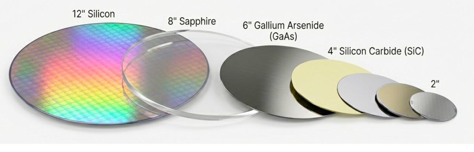
The most widely used substrate in semiconductor fabrication. We supply silicon wafers across the full specification range, from research-grade test wafers to prime-quality production wafers with thermal oxide or thin film coatings.
Type & Orientation
Diameters
Grade
Surface Finish
Resistivity
Flatness & Notch
Wet and dry thermal oxide SiO₂. High-quality gate oxide, isolation, or etch-stop layers. Available on prime wafers.
Thin film deposited wafers available in lots of 25, 50, and 100 wafers. Custom films on request.
Epi silicon on heavily doped substrate. N on N+, P on P+. Custom epi specifications on request.
Glass & Crystalline Substrates:
High performance for a spectrum of applications
Three glass types and three crystalline materials, chosen for optical properties, thermal stability, and chemical resistance. Each serves distinct application domains from displays to UV optics.
BK7 Glass
Renowned for optical applications and exceptional mechanical stability. The standard optical glass, low absorption in the visible spectrum, excellent homogeneity, and easy to polish and coat.
Soda Lime Glass
Valued for ease of fabrication, cost-effectiveness, and versatility for broad applications. The workhorse glass for display and large-format processing, low cost, readily available in large sheets.
Eagle X Glass
Superior quality, clarity, and exceptional durability for specialized applications. Corning Eagle XG, the high-performance flat panel display glass with very low alkali content (EAGLE XG class), which limits ion migration under manufacturer-defined conditions and low thermal expansion coefficient.
Quartz Wafers
High purity, thermally stable, excellent optical and electronic properties with high-temperature resilience. Crystalline quartz for piezoelectric applications and precision optical components.
Fused Silica
Optimal for UV to IR applications due to high transmission and low thermal expansion. The reference material for photomask substrates, deep UV lithography, and precision optical windows.
Sapphire Wafers
Extreme hardness (Mohs 9), broad transparency range, and resistance to both chemical and radiation damage. Substrate of choice for GaN epitaxy (LEDs/HEMTs) and harsh environment devices.
Processing up to 550 × 650 mm
We empower ambitious projects by offering precise processing on glass substrates far exceeding standard wafer diameters. This enables display-panel-scale fabrication, large-format TGV interposers, and glass photomask production in one coordinated process flow.
Advanced Technical Substrates:
Engineered for demanding electronics
SOI, SiC, and piezoelectric substrates, each designed for performance requirements that standard silicon cannot meet. Used in high-frequency RF, power electronics, and precision MEMS.
SOI, Silicon on Insulator
Prominent in electronics for its ability to reduce parasitic device capacitance. The buried oxide layer electrically isolates the active device layer, enabling faster transistors and lower power consumption.
SiC, Silicon Carbide
A powerful combination of high-temperature resistance, high thermal conductivity, and suitability for high-frequency applications. The dominant substrate for EV power devices, industrial inverters, and solar energy systems.
LiNbO₃ & LiTaO₃
Essential for SAW (Surface Acoustic Wave) filters, crucial for telecommunications. Lithium niobate and lithium tantalate are the standard substrates for mobile phone RF front-end filters at 4G/5G frequencies.
Glassy Carbon
A unique combination of chemical inertness, high-temperature stability, and electrical conductivity. The material of choice for electrochemical sensors, bioelectrodes, and harsh chemical environment applications.
Compound & Epi-Wafers:
Next-generation semiconductor devices
III-V compound semiconductors for photonics, RF, and power, materials that silicon simply cannot replicate. Each brings electron mobility, direct bandgap, or breakdown voltage properties beyond silicon's physical limits.
InP, Indium Phosphide
For high-speed electronics and photonics. InP has the very high electron velocity, enabling transistors operating at hundreds of GHz for telecom, radar, and 6G research.
GaAs, Gallium Arsenide
Ideal for LED, laser, and various photonics applications. GaAs was the first direct bandgap semiconductor to enable efficient LEDs. Today it dominates high-brightness LEDs, solar cells, and RF front ends.
GaN, Gallium Nitride
For high-frequency and high-power applications. GaN-on-SiC dominates 5G base station power amplifiers; GaN-on-Si enables cost-effective power transistors for EV chargers and industrial drives.
InGaAs, Indium Gallium Arsenide
For photodetectors and solar cells. InGaAs is the standard near-infrared photodetector material, tunable bandgap by varying In content allows detection from 0.8µm to 3µm, covering all telecom bands.
Material & application matrix find the right substrate instantly
Based directly on our substrate portfolio PDF. Use this matrix to quickly confirm which material suits your device's requirements. Contact us if your combination isn't shown.
| Material | General Purpose | Optical (Visible) | Optical (UV/IR) | High-Frequency | High-Power | High-Temp | Photonic/Laser |
|---|---|---|---|---|---|---|---|
| Silicon | |||||||
| BK7 Glass | |||||||
| Fused Silica | |||||||
| Sapphire | |||||||
| Quartz | |||||||
| SOI | |||||||
| SiC | |||||||
| LiNbO₃ / LiTaO₃ | |||||||
| GaN | |||||||
| GaAs | |||||||
| InP | |||||||
| InGaAs |
Matrix derived from Nanosystems JP Inc. substrate portfolio. ● indicates primary application fit.
Matching substrates to
your device requirements
MEMS Sensors & Actuators
Prime silicon (100) for bulk micromachining, SOI for surface MEMS with isolation, fused silica for low-thermal-noise resonators, quartz for piezoelectric gyroscopes.
Power Devices (EV, Industrial)
4H-SiC for MOSFET and Schottky diodes targeting 650V-10kV. GaN-on-Si for 100-650V power transistors. GaN-on-SiC for RF power amplifiers.
RF & 5G Devices
RF-SOI for antenna switches and tuners. GaAs pHEMT for low-noise amplifiers. InP HEMT for mmWave/THz. LiNbO₃/LiTaO₃ for SAW/BAW filters.
Photonics & Optical
Fused silica for UV to IR optical components. GaAs/InP for laser diodes and VCSELs. InGaAs for photodetectors. Sapphire for GaN LED epitaxy.
Glass Interposers & TGV
Large-format glass (BK7, Soda Lime, Eagle X) up to 550×650mm for TGV interposers. Lower cost and better RF performance than silicon for 2.5D/3D packaging.
Biomedical & Microfluidics
Fused silica for chemically inert microfluidic channels. Glassy carbon for electrochemical bio-sensors and neural recording electrodes. Glass for lab-on-chip diagnostics.
Polyimide film & thin SUS steel
sensor fabrication
Our process capabilities extend to non-wafer flexible and metallic substrates. Photolithography, PVD thin film deposition, and liftoff patterning are available on polyimide (PI) film and thin stainless steel (SUS) foil - enabling thin-film thermocouple fabrication, RTDs, flexible heaters, and precision sensor structures directly on these materials.
Polyimide Film
High-temperature polymer film for flexible sensors, heater patches, and conformal thermocouple arrays. Compatible with photolithography, PVD deposition, and liftoff.
Thin SUS Steel
Stainless steel foil for robust high-temperature thermocouples and strain gauges. Thermally conductive, corrosion-resistant. Requires dielectric isolation layer before sensor deposition.
One substrate foundry
for your entire project
Most substrate sources just ship wafers. We supply substrates as the first step in a complete fabrication project: your substrate spec is confirmed against your downstream process requirements before it's ordered.
4-tier portfolio, one foundry
From standard silicon to GaN epi-wafers, a single purchase order, a single contact, one quality system. No managing multiple substrate sources for different materials in the same project.
Substrate + process in one quote
We confirm your substrate specification against your process flow before ordering, so the resistivity, doping, and surface quality are right for your deposition or etching steps, not just a generic standard spec.
Large-format glass leadership
550×650mm glass substrate processing is rare in Asia. We offer this at both the standard (370×470mm) and full large-format (550×650mm) sizes, enabling panel-scale TGV and display-substrate customers to work with a Japan-based foundry.
🧪 Substrate cleaning: SC1, RCA, and piranha wet chemical cleaning available for all substrate types - including large-format glass panels up to 550×650mm. Supplied standalone or as part of a fabrication engagement.
Cleaning services →Start your project.
Initial response within one business day.
Share your process requirements, substrate, and production volume. A Nanosystems JP Inc. engineer will give an initial response within one business day. Full quote typically within 7-10 business days, subject to project complexity and NDA requirements.