Polyimide Film & Thin
SUS Steel Sensor Fabrication
Standard semiconductor processes - photolithography, thin film deposition, and liftoff - applied to non-wafer flexible and metallic substrates. Enabling thin-film thermocouples, flexible heaters, strain gauges, and precision metallic sensor arrays.
substrate types
& stainless steel
processes
first discussion
Semiconductor precision
on non-conventional substrates
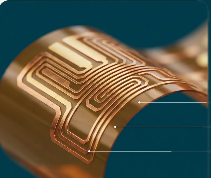
Beyond silicon and glass, Nanosystems JP Inc. has direct process experience applying photolithography, physical vapor deposition, and liftoff patterning to polyimide (PI) films and thin stainless steel (SUS) foils. These are the same processes used on conventional semiconductor substrates - adapted to accommodate the mechanical, thermal, and chemical properties of flexible and metallic materials. The result is precision-patterned thin-film structures directly on substrates that can flex, withstand harsh environments, or integrate into assemblies where a rigid wafer is not an option.
💡 Also on the photolithography page: Direct patterning on PET, PEN, PI (Polyimide), PC (Polycarbonate), PES, COP, and ultra-thin glass substrates up to 400×500mm with 2-3 μm L/S resolution - a complementary flexible substrate capability.
Polymer Film Lithography →Polyimide film & SUS steel
Both materials require process adaptations compared to rigid wafers - but both are well within our established capability range.
Polyimide Film
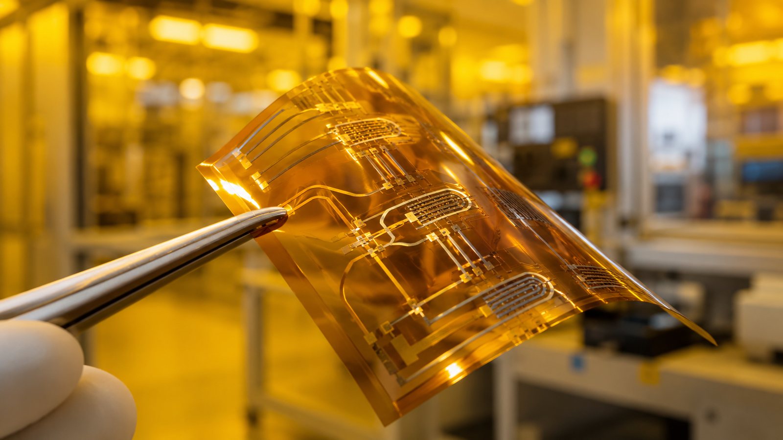
A high-temperature polymer film with exceptional dimensional stability, chemical resistance, and dielectric properties. Widely used in flexible circuits, aerospace sensor patches, and thin-film heater and temperature measurement applications. Standard photolithography and liftoff can be applied directly, provided adhesion and flatness are controlled.
Thin SUS Steel
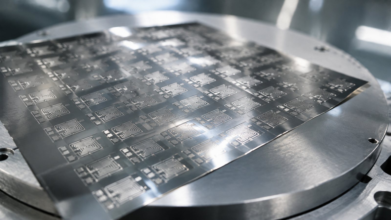
Austenitic stainless steel foil (SUS304, SUS316) provides a robust, thermally conductive, and corrosion-resistant substrate for thin-film sensor structures. Frequently specified for thermocouples and resistive temperature detectors that must survive mechanical contact, elevated temperatures, and aggressive environments where polymer films would degrade.
What works on each substrate
Not every semiconductor process is suitable for flexible or metallic substrates. The table below summarizes what Nanosystems JP Inc. can offer on each material, and where process constraints apply.
| Process | PI Film | SUS Steel | Notes |
|---|---|---|---|
| Photolithography Contact / proximity exposure, positive resist |
✓ | ✓ | Adhesion promoter required on both. PI film must be mounted flat on carrier for processing. |
| PVD Thin Film Deposition Sputtering, e-beam evaporation |
✓ | ✓ | Temperature must be controlled during deposition on PI. Adhesion layers (Ti, Cr) standard on both. |
| Liftoff Patterning Resist-defined metal pattern removal |
✓ | ✓ | Standard liftoff chemistry compatible with both materials. Ultrasonic-free liftoff preferred on thin PI. |
| Wet Etching (acid/base) Chemical subtractive patterning |
✗ | ✓ | Our polyimide route avoids wet etching because strong acids attack PI film; metal wet etch is offered on SUS with appropriate masking. |
| Dry Etching / RIE Reactive ion etching of polyimide film |
✓ | ✗ | RIE / DRIE etching of polyimide film is available - used for via definition, patterning of PI layers, and surface activation. Not applicable to SUS steel. |
| Dielectric Isolation Layer SiO₂ or Al₂O₃ by sputtering |
✓ | ✓ | Required on SUS to electrically isolate the sensor layer from the conductive substrate. Sputtered SiO₂ or Al₂O₃ at low temperature. |
| Dicing / Singulation | ✓ | ✓ | Laser cutting preferred. Blade dicing feasible on SUS. PI may be hand-cut or laser-trimmed for flexible patches. |
Process note: Both polyimide and SUS substrates are processed on a piece-part or sheet basis rather than as round wafers. Substrate handling, mounting, and flatness control are discussed at project scoping. Contact us with your substrate dimensions, thickness, and target process and we will confirm the process sequence.
Thin-film thermocouple
& temperature sensor fabrication
One of the most established applications for photolithography and PVD on flexible and metallic substrates is the fabrication of thin-film thermocouples and resistive temperature sensors. Compared to conventional wire thermocouples, thin-film versions offer faster thermal response, direct substrate integration, and the ability to pattern multiple sensing junctions in a single process run.
Substrate Preparation
Substrate is cleaned, mounted flat on carrier, and an adhesion-promoting or dielectric isolation layer is deposited. On SUS, a thin SiO₂ or Al₂O₃ film electrically isolates the sensor from the conductive base.
Photolithography
Thermocouple junction and lead geometry is patterned in photoresist using contact or proximity exposure. Feature sizes are typically in the range of a few microns to hundreds of microns depending on junction density.
Metal Deposition
Thermocouple leg metals - typically Type K (NiCr/NiAl), Type T (Cu/CuNi), Type E (NiCr/CuNi), or custom alloys - are deposited by PVD (sputtering or e-beam evaporation) through the resist mask or as a blanket film for liftoff.
Liftoff & Inspection
Resist is removed to leave the patterned thermocouple structure. Junction geometry, line width, and continuity are inspected. A protective passivation layer can be added on request for environmental isolation.
Type K, T, E and custom alloy junctions
We work with standard thermocouple alloy pairings - NiCr/NiAl (Type K), Cu/CuNi (Type T), NiCr/CuNi (Type E) - as well as customer-specified metal pairs. Both legs of the junction are patterned on the same substrate in sequential deposition and liftoff steps.
Multi-junction arrays and gradient sensors
Multiple thermocouple junctions can be patterned on a single substrate in a single photolithography pass, enabling spatial temperature profiling, differential temperature measurement, and thermopile configurations for energy harvesting or IR sensing.
Thin, conformal, and embeddable formats
Thin-film thermocouples on PI film can be mounted directly onto curved surfaces, embedded between laminate layers, or bonded onto a device surface - applications where a conventional wire thermocouple would be too bulky, too slow, or mechanically incompatible.
Beyond thermocouples
The same photolithography + PVD + liftoff process sequence used for thermocouple fabrication supports a range of other thin-film sensor and functional device types on flexible and metallic substrates.
Resistive Temperature Detectors (RTD)
Patterned platinum or nickel thin-film resistors on PI or SUS for precision temperature measurement. Higher linearity and repeatability than thermocouple junctions for applications requiring calibrated absolute temperature.
Thin-Film Strain Gauges
Metal foil strain gauges patterned directly on SUS substrates for structural monitoring, force measurement, and pressure sensing in environments where conventional adhesive-bonded gauges are unsuitable.
Flexible Thin-Film Heaters
Patterned resistive heating elements on PI film for uniform area heating, local hot spot generation, or temperature cycling in test fixtures, microfluidic chips, and biological incubation applications.
Antenna & RF Structures on Flexible Substrates
Patterned copper or aluminum traces on polyimide for flexible antenna elements, NFC coils, and RF sensor patches that must conform to a curved or irregular mounting surface.
Biomedical Sensing Patches
Electrode arrays and biosensor structures patterned on flexible PI film for skin-contact, wearable, or implantable sensing applications where conformability and biocompatibility of the substrate are required.
Sensor Integration on Structural Components
Thin-film sensors deposited directly onto SUS structural components - turbine blades, pressure vessel walls, tool surfaces - enabling integrated measurement without an adhesive layer between sensor and structure.
Process experience beyond
the standard substrate list
Hands-on process experience
We have practical fabrication experience on polyimide and SUS substrates, not theoretical compatibility. Process sequences for thermocouple fabrication have been developed and refined on actual substrate samples.
Same process tools as silicon and glass
Photolithography, PVD, and liftoff are applied using the same equipment used for conventional wafer processing. No compromise on feature definition or film quality when moving to flexible or metallic substrates.
Custom alloy and material combinations
We work with thermocouple alloy sputtering targets beyond the most common pairings. If your design specifies a non-standard metal combination, contact us to discuss target availability and deposition conditions.
Small lot, no minimum
Prototype and R&D quantities accepted. Flexible substrate work is often done in small batches - single sheets or a few samples - and we are set up to handle that from the first order.
Tell us about your flexible
or metallic substrate project.
Share your substrate type (PI or SUS), thickness, target pattern geometry, and metal system. A Nanosystems JP Inc. engineer will give an initial response within one business day. Full quote typically within 7-10 business days depending on process complexity and NDA requirements.
sales@nanosystemsjp.co.jp · NDA available on request · Initial response within one business day