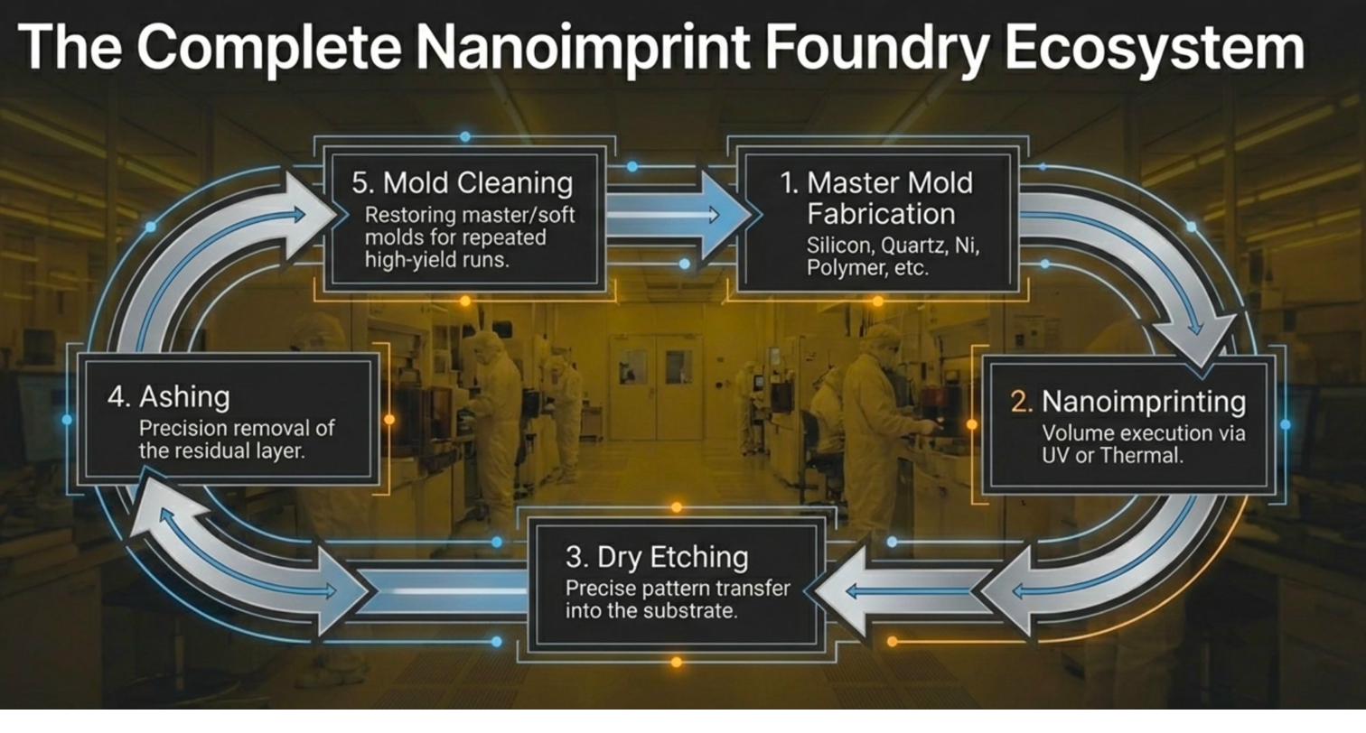
At Nanosystems JP Inc., we offer UV and thermal nanoimprinting and mold fabrication. Nanoimprint lithography transfers a nanopattern from a mold to resist by direct contact, enabling sub-50nm features at far lower cost than e-beam for volume production.
UV Nanoimprinting (UV-NIL)
Soft polymer mold pressed into UV-curable resist, exposed by UV, then demolded. The soft mold protects the expensive master across thousands of imprint cycles, essential for volume production. High refractive index (high-n) NIL resist available for optical waveguides, metasurface lenses, and anti-reflection structures. Large substrate capability to approximately 500×500mm.
Thermal Nanoimprinting
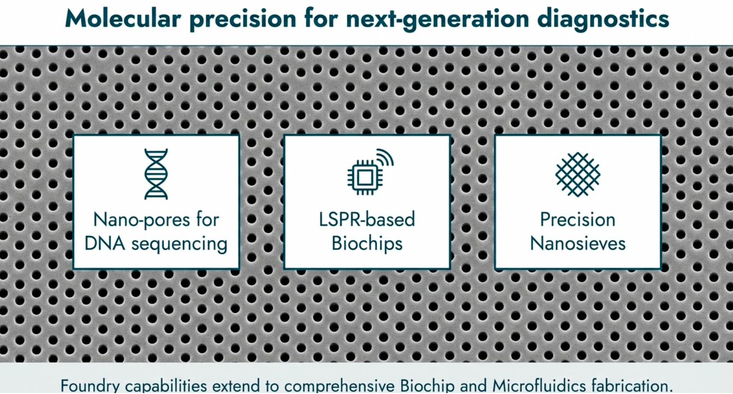
Substrate heated above glass transition temperature, hard mold pressed in, cooled, demolded, no UV required. Works directly on PMMA, PC, and PET thermoplastic substrates without any resist coating step. The most direct route to nanopatterned polymer biochips, optical diffusers, and display optical films. Also used to replicate nanostructures into polymer substrates during injection molding.
Master Mold Fabrication
We fabricate the master mold itself, silicon (e-beam direct-write + DRIE), quartz (e-beam + etch), nickel (electroformed from Si master), or polymer. At Nanosystems JP Inc., we handle mold creation, NIL, dry etch, and ashing as a single coordinated flow. Critical for IP protection: your nanoscale pattern design stays with us from first design through to finished chip.
Post-Imprint Processing
Complete integration after NIL: dry etching to transfer the imprinted pattern into the substrate material (Si, SiO₂, glass), O₂ plasma ashing to remove the thin residual NIL resist layer that remains after demolding, and mold cleaning protocols to preserve mold lifetime across hundreds to thousands of imprint cycles.
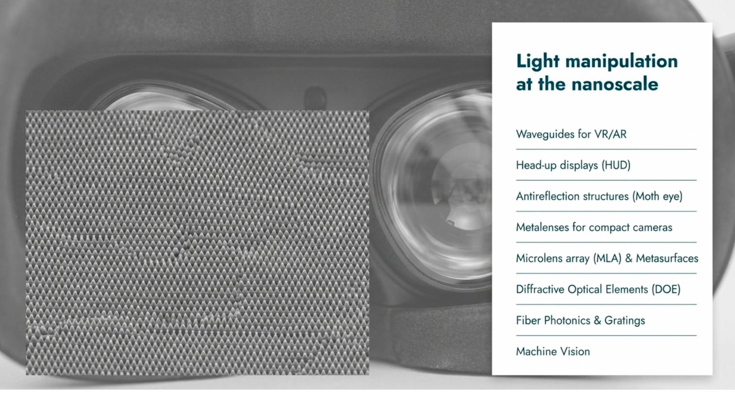
High-n Resist for Photonics
Specialist high refractive index (high-n) NIL resist for fabricating optical waveguides, metasurface lenses, and anti-reflection moth-eye structures. The high refractive index contrast between the imprinted structure and surrounding medium enables strong optical guiding, diffraction, and reflection control, critical for AR/VR waveguide gratings and LiDAR optical elements.
Large-Area UV-NIL
UV-NIL on substrates up to approximately 500×500mm, enabling large-area microlens arrays, display optical films, and panel-scale biochip substrates that 4-6 inch wafer NIL tools cannot process. Large-area NIL is particularly important for display optics (anti-glare, brightness enhancement), solar cell texturing, and biochip array substrates where large format is required for cost-effective chip production.