Application-Specific Fabrication

Biochip & Microfluidic
Chip Fabrication

At Nanosystems JP Inc., we offer full-service biochip and microfluidic chip fabrication on glass, silicon, and polymer substrates. 500×600mm large-format glass processing for low cost-per-chip on biosensor arrays. NIL for sub-50nm nanopores and LSPR structures. PDMS soft lithography for organ-on-chip. DRIE for Bio-MEMS. All bonding methods .

Glass 500×600mm Borosilicate · Quartz Silicon DRIE 50:1 PDMS soft lithography PC · COP · PMMA NIL nanopores <50nm LSPR Au nanostructures Au · Pt · ITO electrodes
3
Substrate families:
glass, silicon, polymer
500×600mm
Max glass panel lowest chip cost
<50nm
NIL nanopores &
LSPR structures
6
Bonding methods
for chip sealing
Three Substrate Families
Glass, silicon, and polymer each with distinct advantages

The substrate defines fabrication route, optical properties, chemical resistance, thermal stability, cost, and biocompatibility. We fabricate on all three, and build hybrid chips combining two.

Glass

Up to 500×600mm · Borosilicate · Quartz · Fused Silica
Optically transparent Chemically inert Hermetic bonding

Glass is the workhorse substrate for high-performance microfluidic chips: optically transparent for fluorescence imaging and absorbance measurement, chemically inert to acids, bases, and solvents that dissolve PDMS, and compatible with high-temperature sterilisation. Our 500×600mm large-format glass processing enables more chips per run than any wafer-format foundry, dramatically reducing cost-per-chip for array biosensors and diagnostic plates.

Standard glass materials: borosilicate (Eagle XG, Pyrex), quartz (UV-transparent for 200nm excitation), fused silica (lowest autofluorescence), and soda lime (lowest cost for disposable chips). Channels and features defined by HF wet etching (isotropic, rounded profile), laser ablation, or ICP-RIE (anisotropic, vertical walls). Thin film electrode deposition of Au, Pt, ITO, TiN available on the same substrate before bonding.

500×600mm panel Borosilicate · Quartz · Fused silica HF wet etch, isotropic channels ICP-RIE, vertical walls Au · Pt · ITO electrodes Anodic / fusion bonding

Silicon

4–12 inch · DRIE 50:1 · TSV feedthroughs · Bio-MEMS
High-aspect-ratio DRIE CMOS-compatible TSV integration

Silicon offers capabilities unavailable in glass or polymer: DRIE creates high-aspect-ratio channels, pillars, and filter structures with perfectly vertical sidewalls at 50:1 aspect ratio, enabling size-based cell sorting, deterministic lateral displacement arrays, and nanofluidic confinement that polymer chips cannot achieve. Silicon also enables on-chip CMOS readout integration via TSV, connecting microfluidic sensors to signal conditioning circuits on the same die.

Standard semiconductor lithography (KrF stepper, mask aligner) provides sub-1µm feature resolution. Thin film piezoelectric (PZT, AlN) and electrode materials are deposited on the same silicon substrate, enabling acoustic actuation, DEP trapping, and electrochemical detection. Glass-on-silicon hybrid chips (glass cover bonded anodically to Si channel layer) provide optical access through the glass while retaining silicon's structural precision.

DRIE 50:1 aspect ratio KrF / mask aligner litho TSV CMOS integration PZT · AlN piezoelectric Cell sorting · DLD arrays Glass-on-Si hybrid chips

Polymer

PDMS · PC · COP · PMMA · SU-8
Lowest cost Soft lithography Injection molded

Polymer chips dominate biomedical research and point-of-care diagnostics, not because they are technically superior, but because they are cheap, fast to prototype, and disposable. PDMS (polydimethylsiloxane) is the gold standard for research: bonded to glass or another PDMS layer by O₂ plasma activation, it forms the channels of organ-on-chip devices, droplet generators, and pneumatic valve arrays (Quake valves) within days of design iteration.

For production volumes, injection-molded PC, COP, and PMMA chips provide the same geometry at lower cost than PDMS casting. COP (cyclo-olefin polymer) has negligible autofluorescence, critical for fluorescence-based assays where PDMS background interferes with detection. Thermal NIL on PMMA replicates nanostructures (gratings, nanopores, LSPR features) directly into polymer substrates for combined micro-nano chips.

PDMS soft lithography SU-8 master mold PC · COP · PMMA molding Thermal NIL on PMMA Quake pneumatic valves Low autofluorescence COP
Fabrication Techniques
Every technique needed for
micro-to-nano scale biochips

Biochip fabrication combines lithography, etching, thin film deposition, replication, and bonding, often on the same chip. All techniques are available , coordinated in a single project.

Building the Biochip: From Substrate to Sensing Layer - exploded 4-layer diagram showing microfluidic interface, active circuitry and electrodes, vias and interconnects, and base substrate
💡

Photolithography

E-beam (20nm), KrF stepper (50nm, up to 12 inch), mask aligner (4µm, up to 500×600mm), and polymer film lithography (PET/PEN, 400×500mm). Front-to-back alignment for double-sided microfluidic structures. SU-8 thick photoresist (up to 500µm) for tall MEMS channel walls and master molds for PDMS soft lithography. Large-format mask aligner processes glass biochip arrays at 500×600mm in a single step.

E-beam 20nm KrF 50nm / 12″ Mask aligner 500×600mm SU-8 up to 500µm thick Front-to-back align
⚗️

Wet & Dry Etching

HF etching of borosilicate and quartz glass for isotropic rounded microchannels, the standard for glass electrophoresis and DNA separation chips. KOH and TMAH anisotropic etching of silicon for V-groove and pyramidal structures. DRIE for high-aspect-ratio Si channels, through-holes, and micropillar filter arrays up to 50:1. ICP-RIE for glass and quartz with near-vertical sidewalls. Wet KOH etching with TMAH produces smooth <0.5nm Ra channel surfaces for single-molecule nanofluidics.

HF glass, isotropic channels KOH · TMAH Si etch DRIE 50:1 aspect ratio ICP-RIE glass, vertical walls Ra <0.5nm nanofluidics
🔬

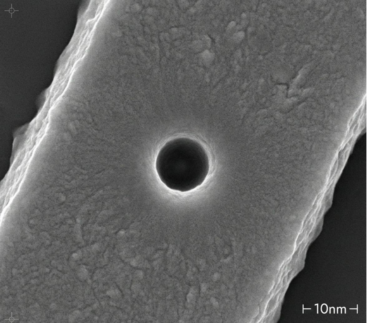
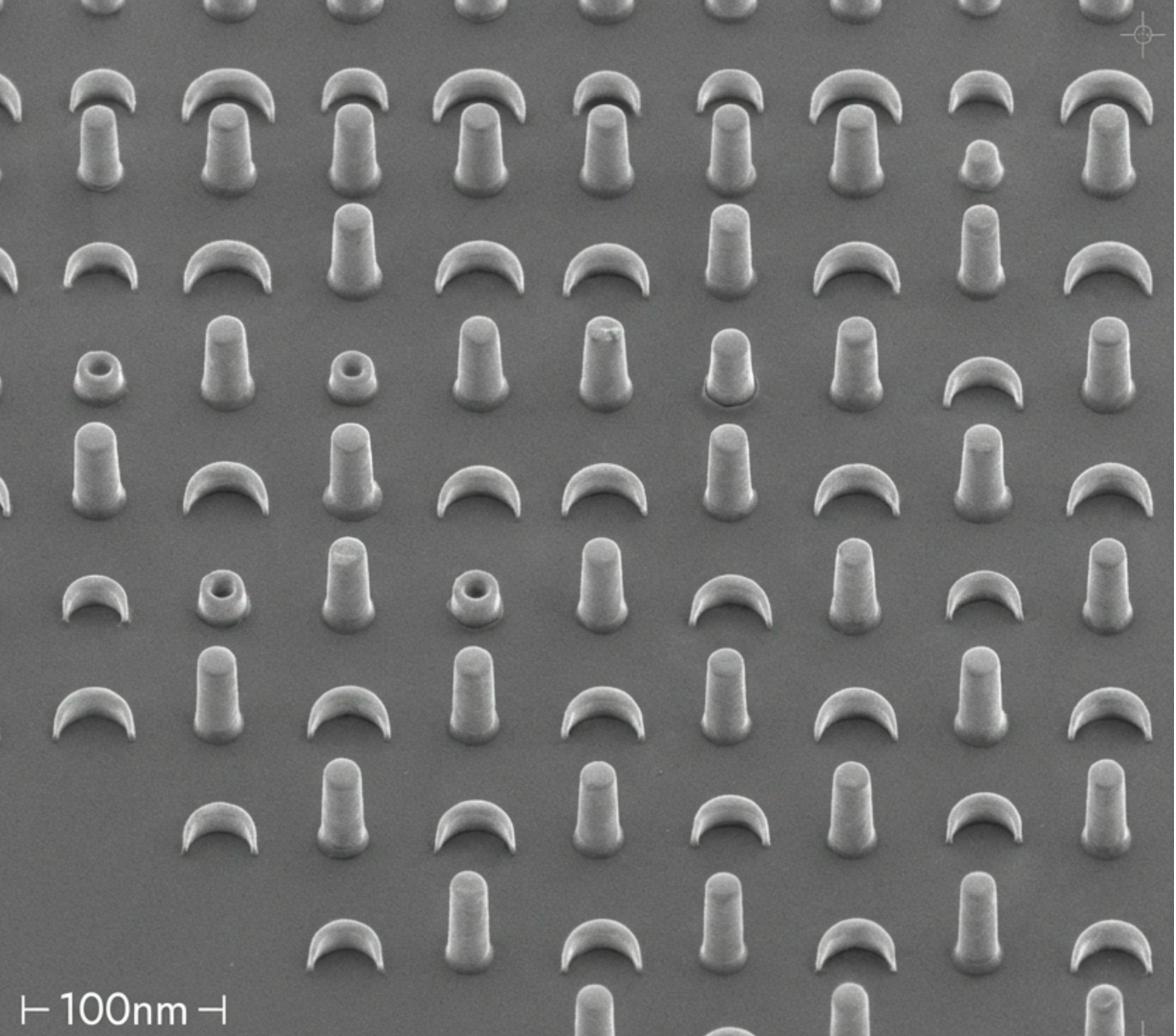
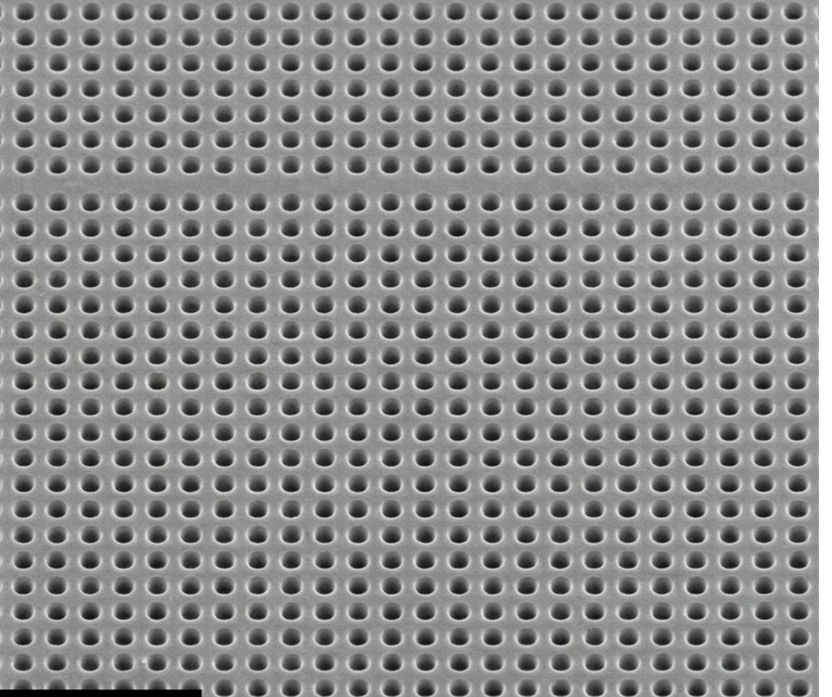
Nanoimprinting (NIL)

UV and thermal nanoimprint lithography for sub-50nm nanostructures integrated into biochip substrates. DNA sequencing nanopore arrays: NIL defines the nanopore geometry in resist, dry etch transfers to SiN membrane. LSPR biosensor chips: NIL patterns gold nanopillar or nanohole arrays for label-free plasmon-resonance sensing. Thermal NIL on PMMA for polymer biochips with nanofluidic confinement channels. Master mold fabrication (Si e-beam, Ni electroformed) .

UV-NIL soft mold Thermal NIL, PMMA DNA nanopores <50nm LSPR Au nanostructures Si/Ni master molds

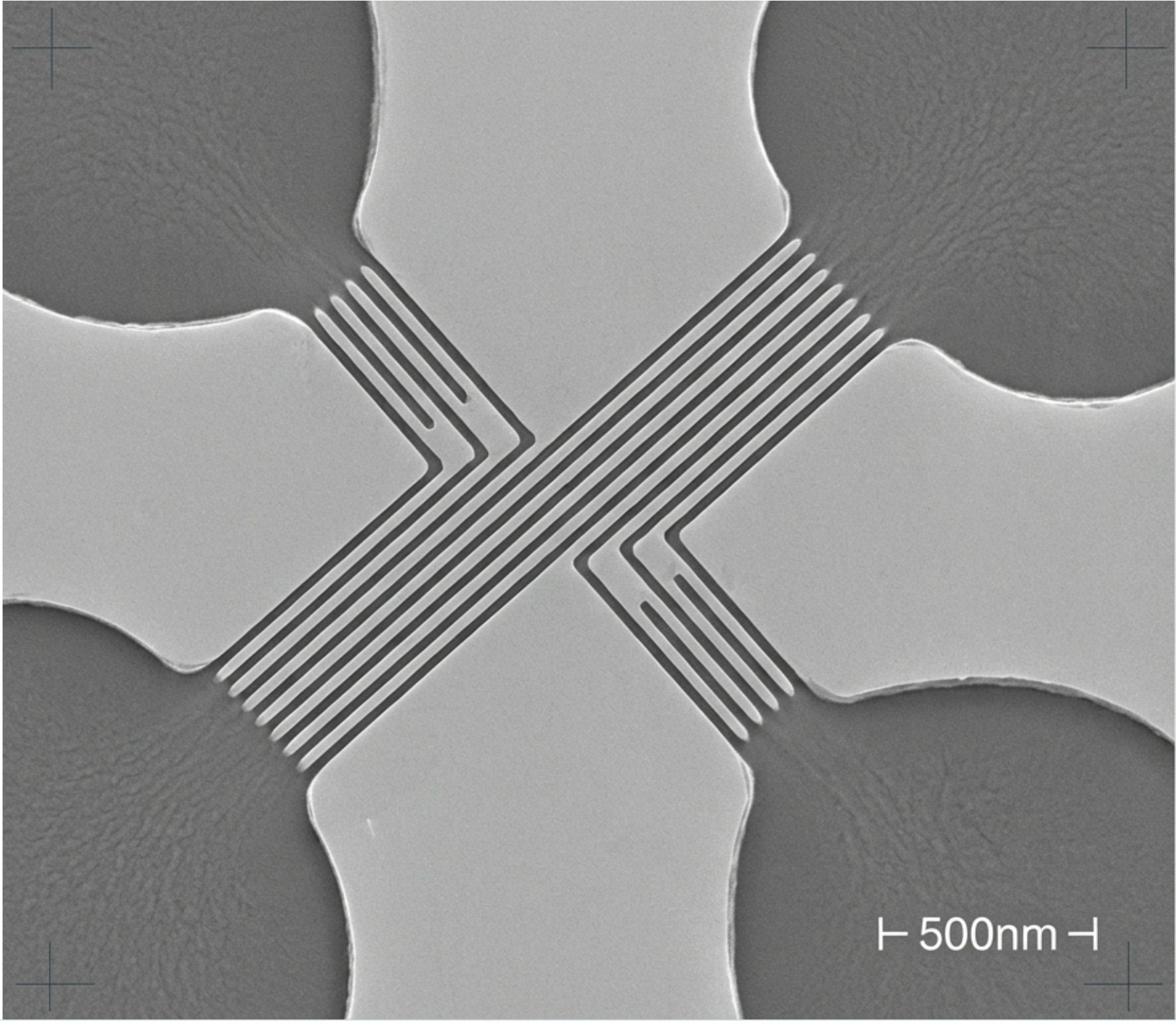
Thin Film Deposition Electrodes

Biocompatible electrode metals deposited by PVD sputtering and e-beam evaporation: gold (Au) for thiol-chemistry biofunctionalization, platinum (Pt) for electrochemical detection and electroporation, ITO (indium tin oxide) for transparent electrodes compatible with optical detection through the electrode, and TiN for capacitive sensing. Lift-off patterning defines electrode arrays with sub-5µm features. Multi-electrode arrays (MEA) for neural recording chips fabricated on glass or Si substrates.

Au, thiol biofunctionalization Pt, electrochemical ITO, transparent electrode TiN, capacitive sensing Lift-off, sub-5µm features MEA for neural chips
🧪

PDMS Soft Lithography

The standard rapid-prototyping route for research-grade microfluidic chips. SU-8 photolithography on a silicon wafer defines the channel master mold, channel heights from 5µm to 500µm. Liquid PDMS is poured over the master, degassed, cured at 70°C, and peeled off, producing a negative replica of the channels in transparent, flexible PDMS. Multiple PDMS layers are bonded by O₂ plasma activation to create three-dimensional channel networks, pneumatic valves (Quake valve architecture), and organ-on-chip structures. Design-to-first-chip turnaround: 3–5 days.

SU-8 master on Si Channel height 5–500µm O₂ plasma bonding Quake pneumatic valves 3–5 day turnaround Organ-on-chip capable
🏭

Injection Molding & Thermal NIL

For production volumes (thousands to millions of chips), injection molding of PC, COP, and PMMA produces biochip substrates at cents-per-chip, far below the cost of individually cast PDMS or etched glass chips. We fabricate the injection mold tooling (Si or Ni master) . Thermal NIL on PMMA replicates nanoscale features (100nm–5µm gratings, nanopore templates, nanowell arrays) directly during molding, combining micro and nano features in a single fabrication step.

PC · COP · PMMA molding Si / Ni mold tooling Thermal NIL on PMMA Nanofeatures during molding Production scale
Nanoscale Bio Structures
Sub-50nm structures for DNA,
single molecules, and plasmonics

Biochip applications increasingly require nanoscale features invisible to standard UV lithography. Our NIL and e-beam capabilities bring sub-50nm resolution to biochip fabrication at production-relevant scales.

Nanoscale capability for biochips
The nanoscale is where biology happens, and where most foundries stop
DNA is 2nm wide. Proteins are 5–50nm. Ion channels are <1nm. Making biochips that interact with biology at its native scale requires nanofabrication, not just microfluidics. Our NIL, e-beam, and DRIE capabilities enable nanostructures integrated directly into microfluidic chips, without shipping substrates to a separate nanofabrication facility.
SEM micrograph of a DNA nanopore - 10nm scale freestanding SiN membrane nanopore, 5-50nm diameter
🧬
DNA Nanopores
Geometry5–50 nm diameter
MaterialFreestanding SiN or Si₃N₄ membrane
ApplicationUniform pore arrays for nanopore sequencing and molecular sieving
SEM micrograph of LSPR nanostructures - Au pillars, holes, and crescents at 50-200nm scale patterned by NIL and lift-off, 100nm scale bar
🔆
LSPR Nanostructures
GeometryAu pillars, holes, and crescents at 50–200 nm
MethodologyPatterned by NIL and lift-off
ApplicationLocalised surface plasmon resonance for label-free biosensing. Antibody or aptamer functionalised for protein or nucleic acid detection
SEM micrograph of nanofluidic channels - sub-100nm channel depth, 500nm scale bar, defined via e-beam lithography and DRIE
🔵
Nanofluidic Channels
GeometrySub-100 nm channel depth
MethodologyDefined via e-beam lithography and DRIE
ApplicationConfinement channels for single DNA molecule stretching, entropy-reduction mapping, and nano-coulter counters for nanoparticle detection
SEM micrograph of nanowell array - femtolitre-volume uniform wells in PMMA or COP, millions of wells per chip patterned by NIL
🔴
Nanowell Arrays
GeometryFemtolitre-volume defined in PMMA or COP
MethodologyNIL on polymer
ApplicationDigital ELISA single-molecule enzyme assays. Millions of wells per chip achieved at production cost
NIL master mold fabrication , Si e-beam and Ni electroformed
Sub-50nm nanopores for nanopore sequencing applications
LSPR gold nanostructure arrays: pillars, holes, crescents
Nanofluidic channel integration alongside microfluidic channels
Thermal NIL on PMMA for polymer nanowell arrays
E-beam direct-write for custom nanoscale geometries (no mask)
SiN membrane fabrication for nanopore and nanomechanical sensors
Pattern transfer to glass, Si, and polymer substrates
Chip Sealing & Bonding
Six bonding methods, matched
to your substrate combination

Bonding seals the microfluidic channels and is the step that most often determines chip yield. The wrong bonding method causes channel collapse, delamination, or optical scattering. We offer every relevant bonding method , matched to the substrate combination and application requirement.

PDMS ↔ Glass
O₂ plasma activation of both surfaces followed by contact bonding. The industry standard for lab-on-chip research devices. Optically clear, biocompatible, and reversible before plasma activation, enabling chip inspection and testing before permanent seal. Bond strength: ~200kPa burst pressure.
O₂ plasmaOptically clearResearch standard
PDMS ↔ PDMS
Plasma bonding of two PDMS layers for multilayer microfluidic chips. Enables Quake-valve pneumatic control channel networks above fluidic channels. Critical for organ-on-chip devices with separate media and air/vacuum control circuits. Thin PDMS membranes (5–20µm) form the valve diaphragm.
O₂ plasmaMultilayerQuake valves
PDMS ↔ SUS / Metal
PDMS bonded to stainless steel or aluminium backing for robust, reusable microfluidic fixtures. Metal backing provides mechanical rigidity for pressure-tolerant flow cells, electrophoresis clamps, and portable diagnostic devices that cannot use fragile glass or flexible PDMS-only chips.
Adhesive layerRobustReusable
Glass ↔ Silicon (Anodic)
Anodic bonding at 250–450°C under electrostatic field, creates true hermetic glass-Si seals without intermediate adhesive. The standard for MEMS microfluidic sensors, pressure sensors integrated into flow channels, and glass-capped Si DRIE chips requiring autoclave sterilisation compatibility. Triple-stack glass-Si-glass available.
250–450°CTrue hermeticAutoclave-compatible
Glass ↔ Glass (Fusion)
Plasma-activated direct fusion bonding of glass-to-glass for the cleanest possible optically transparent chips, no adhesive layer in the optical path. Surface roughness must be <0.5nm Ra (CMP-polished) before bonding. Used for DNA sequencing flow cells, high-pressure capillary electrophoresis chips, and UV-excited fluorescence chips where any adhesive autofluorescence is unacceptable.
Plasma-activatedNo adhesiveUV-transparent
PC / COP / PMMA Thermal
Thermal bonding of rigid thermoplastic chips by pressing slightly above glass transition temperature, fusing the two halves without adhesive. Compatible with injection-molded chips where adhesive residue in channels would interfere with surface chemistry or clog nanoscale features. UV adhesive bonding available for lower-temperature polymers.
Thermal pressNo adhesiveInjection molded
Substrate Comparison
Glass, silicon, and polymer key parameters side by side
ParameterGlassSiliconPolymer (PDMS/PC/COP)
Max Substrate Size500×600mm panelUp to 12 inch (300mm)PDMS: cast; Mold: up to 12 inch
Channel PatterningHF wet etch, ICP-RIE, laserDRIE (50:1), KOH, TMAHSoft litho (PDMS), injection mold, NIL
Min Feature Size~2µm (ICP-RIE)~0.5µm (DRIE)~5µm (mold); <100nm (NIL)
Optical TransparencyExcellent (UV to NIR)Opaque (IR only)PDMS: excellent; COP: very good
Chemical ResistanceExcellent, inert to most solventsExcellent (oxide passivated)PDMS: swells in organics; COP: good
BiocompatibilityExcellent, ISO 10993Good (oxide surface)PDMS: excellent; PI grade PI: ISO 10993
Thermal StabilityUp to 600°C (quartz)Up to 1000°CPDMS: to 200°C; PI: to 400°C
Electrode IntegrationAu, Pt, ITO, direct depositionAu, Pt, TiN, standard CMOSLimited, low-temp metals only
CMOS IntegrationVia TSV in hybrid chipNative, same waferNo
Bonding MethodsAnodic, fusion, adhesiveAnodic (to glass), fusionO₂ plasma (PDMS), thermal (PC/COP)
Cost (per chip)Medium, low at 500×600mm scaleMedium–highLowest (PDMS research; mold: very low)
Prototype Turnaround1–3 weeks2–4 weeksPDMS: 3–5 days; mold: 4–8 weeks
Applications
Life sciences, diagnostics,
and biomedical devices
🧬

DNA Sequencing Flow Cells

Glass flow cells with NIL-defined nanopore arrays and precision microchannels for nanopore sequencing and optical sequencing platforms. Fusion or anodic bonding provides the hermetic seal and UV transparency required. Large-format glass processing enables 96-well or 384-well array formats at competitive cost.

Glass fusion bond · NIL nanopores · 500×600mm · UV-transparent
🏥

Point-of-Care Diagnostics

COP injection-molded chips for lateral flow assay, RT-PCR, immunoassay, and CRISPR-based diagnostics. COP's low autofluorescence enables fluorescence readout. PDMS prototyping to injection-molded production, same design file, different material. Thousands to millions of chips per batch at production cost.

COP injection mold · LFA · RT-PCR · CRISPR assay · Low autofluorescence
🫀

Organ-on-a-Chip / OOC

Multilayer PDMS chips with Quake pneumatic valves, peristaltic pumps, and mechanical stretch membranes for microphysiological systems, lung, gut, blood-brain barrier, and kidney-on-chip. PDMS-to-PDMS plasma bonding creates three-dimensional vascular and tissue channel networks. COP versions available for mass production.

PDMS multilayer · Quake valves · Pneumatic stretch · OOC / MPS
🔆

LSPR Label-Free Biosensors

Gold nanostructure arrays (nanopillars, nanoholes, nanoslits) on glass substrates by NIL and lift-off. Surface functionalised with antibodies, aptamers, or nucleic acid probes. Localised surface plasmon resonance detects binding of target molecules, protein, nucleic acid, or small molecule, without fluorescent labels. For clinical diagnostics and drug discovery.

NIL + Au lift-off · LSPR · Label-free · Antibody / aptamer probe

Cell Sorting & DEP Trapping

Silicon DRIE micropillar arrays for deterministic lateral displacement (DLD) size-based cell sorting. ITO or Pt electrode arrays on glass for dielectrophoretic (DEP) trapping and manipulation. Tumour cell isolation from blood, circulating tumour DNA (ctDNA) concentration, and rare cell analysis for liquid biopsy applications.

DRIE micropillars · DLD · DEP electrodes · ITO/Pt · Liquid biopsy
🧠

Neural Recording Chips (MEA)

Multi-electrode arrays (MEA) for neural signal recording and stimulation, Pt or TiN electrodes on glass or Si substrate, passivated with SU-8 or polyimide, with DRIE through-holes for neuron interface. Biocompatible polyimide RDL for flexible implantable probe variants. For brain-computer interface research and epilepsy monitoring.

Pt / TiN MEA · SU-8 passivation · DRIE · PI RDL · BCI
🔬

Single-Molecule Analysis

E-beam patterned nanofluidic channels (<100nm depth) for DNA stretching and single-molecule fluorescence mapping. Zero-mode waveguides (ZMW) patterned by e-beam or NIL in gold film for single-molecule sequencing by synthesis. Nanowell arrays (femtolitre volume) for digital ELISA and single-enzyme assays.

E-beam <100nm channels · ZMW in Au film · Nanowell arrays · Digital ELISA
💉

Drug Delivery & Microencapsulation

PDMS and glass droplet microfluidic chips for monodisperse emulsion generation, microencapsulation, and drug-loaded microsphere production. T-junction and flow-focusing geometries produce droplets from 5µm to 500µm with CV <2%. Glass chips preferred for surfactant-tolerant surfaces and elevated temperature operation.

PDMS / glass · Droplet microfluidics · T-junction · Flow focusing · CV <2%
🧫

Cell Culture & Perfusion

Large-format glass multi-well plates and flow-through cell culture chambers, processed on 500×600mm glass panels for cost-effective production of multi-channel cell culture arrays. Integrated Au or ITO electrodes for transepithelial electrical resistance (TEER) measurement. SU-8 cell culture scaffold structures for 3D spheroid culture.

500×600mm glass · Multi-well plates · Au/ITO TEER · SU-8 3D scaffold
Why Nanosystems JP Inc.
What makes our biochip capability
different
01

500×600mm glass, lowest chip cost

Processing biochip substrates at 500×600mm panel scale produces far more chips per run than 4- or 6-inch wafer formats. For array biosensors and diagnostic plates with hundreds of chips per substrate, this single capability can reduce chip cost by 5–10× compared to wafer-scale foundries.

02

Nano to micro, one coordinated process flow

Sub-50nm NIL nanopores integrated into microfluidic chips without shipping the substrate to a separate nanofab. E-beam direct write for custom nanoscale geometries. Nanofluidic + microfluidic hybrid chip design is handled by one engineering team with a single project timeline.

03

All three substrate families

Glass for optical biochips, silicon for Bio-MEMS and CMOS integration, PDMS for soft lithography prototypes, COP/PC/PMMA for injection-molded production. The material choice is driven by your device requirement, not by what the foundry happens to process.

04

PDMS to production, same design

Prototype in PDMS (3–5 day turnaround), then transition to injection-molded COP or PC with the same channel design. Mold tooling fabricated . No redesign for a different foundry's process, your channel geometry transfers directly from soft lithography to molded production.

05

All bonding methods

O₂ plasma for PDMS-glass and PDMS-PDMS, anodic for glass-Si hermetic, fusion for glass-glass UV-transparent, thermal for PC/COP, all six bonding methods available. No separate bonding vendor for the chip sealing step. Bond quality verified by optical inspection and leak testing before delivery.

06

NDA available on request

Biochip designs - channel layouts, electrode geometries, surface chemistry protocols, and assay designs - represent years of development. An NDA can be arranged before any design files or technical details are shared - just mention it in your first message. Initial inquiries and quotes can proceed without one. Pure-play foundry: we do not develop competing biochip products.

Related service

AuSn Bump Services: For photonic biochips requiring flip-chip assembly of laser sources or photodetectors, our AuSn bump service provides hermetic fluxless bonding at wafer scale.

AuSn Bump Services →

Start your project.
Response within 1 business day.

Share your process requirements, substrate, and production volume, A Nanosystems JP Inc. engineer will respond within 1 business day. Full quote typically within 7–10 business days, subject to project complexity and NDA requirements.

[email protected] · +81-3-5288-5569 · NDA available on request

All Services
Full process flow →
Substrates
🔷 Substrate & WafersSi, SiC, GaN, glass, sapphire 🔬 Fused Silica WafersQuartz · borosilicate · low CTE 🟣 PI Film & SUS Sensor FabRoll-to-roll · sensor patterning
Front-End
🎭 Mask FabricationGDS to chrome mask, DRC 💡 PhotolithographyE-beam 20nm to 500×600mm 🔬 NanoimprintingUV & thermal NIL 🔵 Thin Film DepositionPVD, CVD, ALD, MBE ⬆️ LiftoffMetal pattern · shadow mask ⚡ ElectroplatingCu TSV fill, DPC, LIGA ⚗️ EtchingICP-RIE, DRIE >50:1 🌡️ AnnealingN₂/H₂/vacuum/RTA 🎯 Ion ImplantationB/P/As/Al/N implant 🔶 CMP & GrindingCu CMP, 50µm thinning ✂️ DicingBlade, stealth laser 🧪 Wafer CleaningRCA, plasma, megasonic
Advanced Packaging
🔗 Wafer BondingHybrid, eutectic, fusion 📌 TSV FabricationHigh AR, void-free Cu fill 🔓 TSV RevealBackgrind → etch → CMP 🪟 TGV FabricationThrough-glass via 📐 RDL FabricationBCB/PBO/PI + damascene 📦 Packaging & AssemblyWire bond, flip-chip 📚 3D/2.5D PackagingTSV+RDL+UBM+C4 🥇 AuSn BumpPVD lift-off, fluxless 🧬 Biochip & MicrofluidicsGlass 500×600mm, NIL 🔆 SiPho PackagingTSV·RDL·UBM·C4 for PIC
Industries
🤖 AI & HPC PackagingCoWoS-style, 2.5D/3D 💎 Silicon PhotonicsSOI · AuSn · TSV interposer 🚗 AutomotiveMEMS sensors, SiC power 🧬 Life SciencesLab-on-chip, biosensors 🔭 All Industries → Request a Quote →
Technical AI — Nanosystems JP Inc.
Online — typically replies in minutes
Services & Industries
⚙️ Capabilities Overview
Substrates
🔷 Substrate & WafersSi, SiC, GaN, glass, sapphire 🔬 Fused Silica WafersQuartz · borosilicate · low CTE 🟣 PI Film & SUS Sensor FabRoll-to-roll · sensor patterning
Front-End
🎭 Mask FabricationGDS to chrome mask, DRC 📷 PhotolithographyE-beam 20 nm to 500×600 mm 🔬 NanoimprintingUV & thermal NIL 🫧 Thin Film DepositionPVD, CVD, ALD, MBE ⬆️ LiftoffMetal pattern · shadow mask ⚡ ElectroplatingCu TSV fill, DPC, LIGA 🌊 EtchingICP-RIE, DRIE >50:1 🔥 AnnealingN₂ / H₂ / vacuum / RTA ⚛️ Ion ImplantationB / P / As / Al / N implant 🔄 CMP & GrindingCu CMP, 50 µm thinning 💎 DicingBlade, stealth laser 🧪 Wafer CleaningRCA, plasma, megasonic
Advanced Packaging
🔗 Wafer BondingHybrid, eutectic, fusion 📌 TSV FabricationHigh AR, void-free Cu fill 👁️ TSV RevealBackgrind → etch → CMP 🪟 TGV FabricationThrough-glass via 🔀 RDL FabricationBCB / PBO / PI + damascene 📦 Packaging & AssemblyWire bond, flip-chip 📚 3D / 2.5D PackagingTSV + RDL + UBM + C4 🥇 AuSn BumpPVD lift-off, fluxless 🧬 Biochip & MicrofluidicsGlass 500×600 mm, NIL 🔆 SiPho PackagingTSV · RDL · UBM · C4 for PIC
Industries
🤖 AI & HPC PackagingCoWoS-style, 2.5D / 3D 💡 Silicon PhotonicsSOI · AuSn · TSV interposer 🚗 AutomotiveMEMS sensors, SiC power 🧬 Life SciencesLab-on-chip, biosensors 🔭 All Industries → Request a Quote →