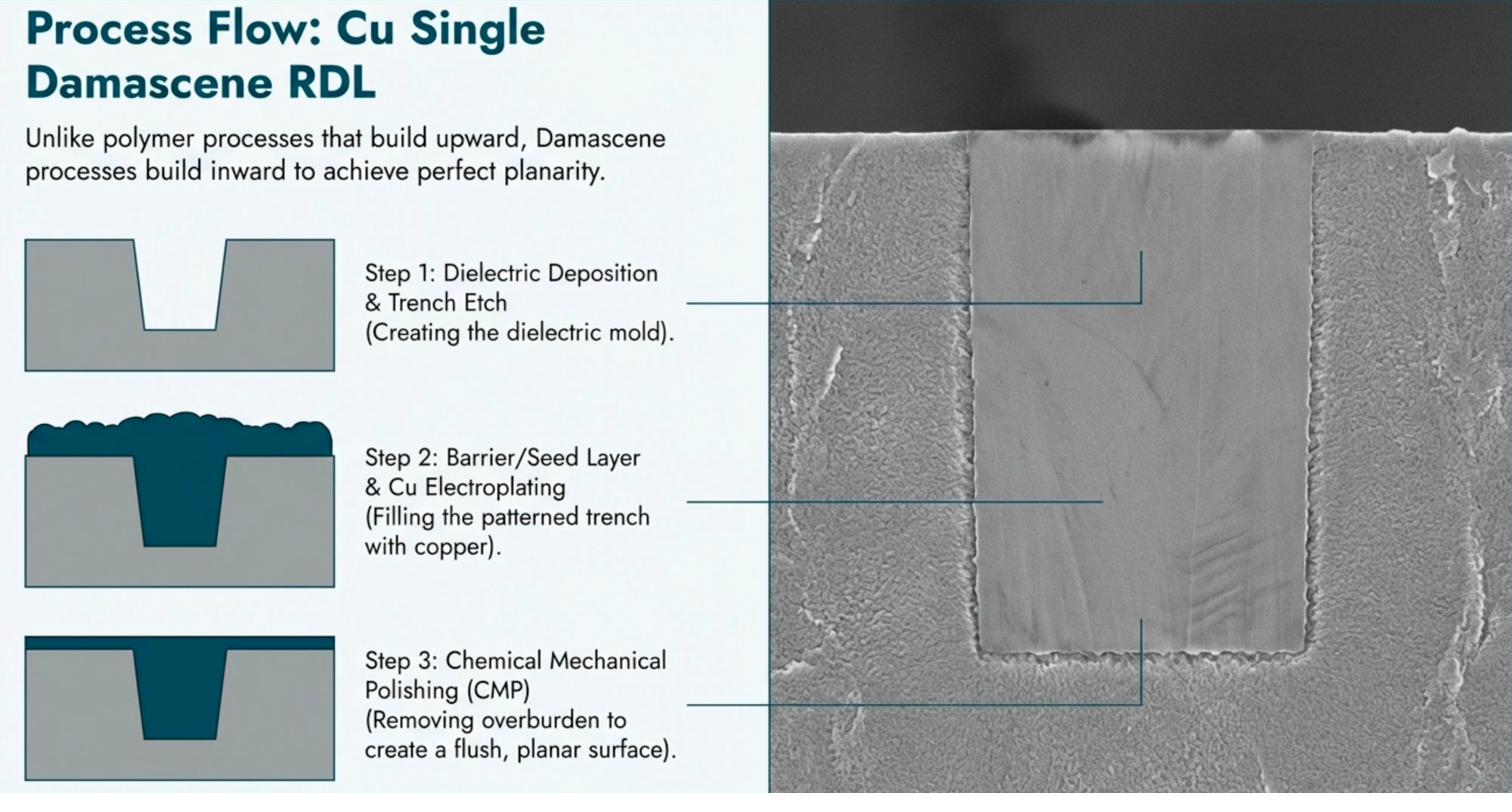
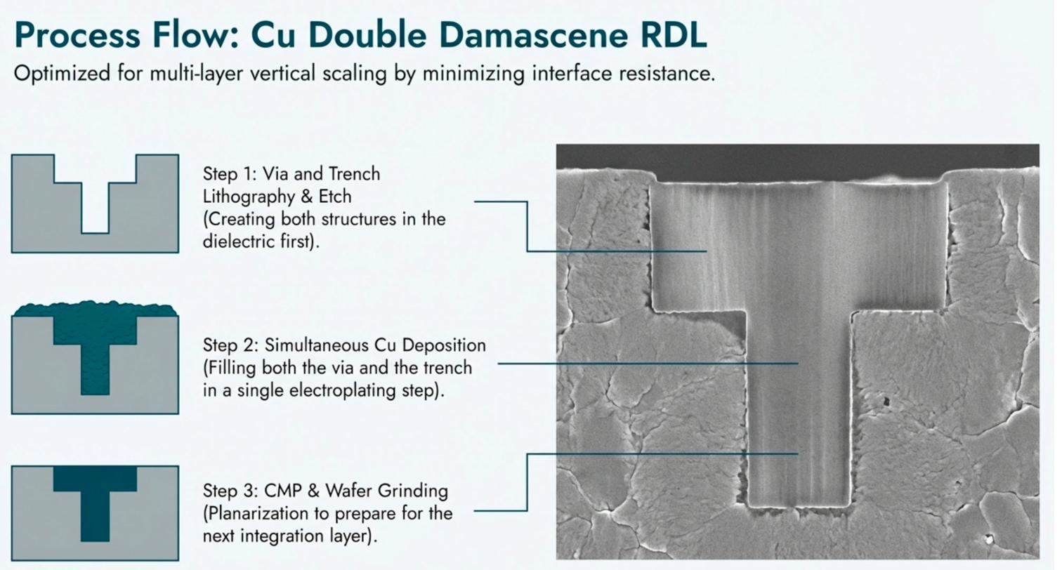
At Nanosystems JP Inc., we offer two complete RDL routes - polymer passivation (BCB, PBO, PI) and Cu damascene - for redistributing chip I/O from device pad pitch to package bump pitch, enabling fan-in and fan-out wafer-level packaging. Both routes are available as standalone processes or as part of a full TSV → RDL → UBM → C4 bumping flow, with integrated backgrinding, dicing, and flip-chip assembly.
Device pads on a finished wafer are typically at a pitch of 50–150µm, too tight for direct solder bumping at board assembly. RDL fabricates one or more layers of metal interconnect on top of the completed wafer to reroute these pads to a wider, solderable bump pitch, or to extend the I/O footprint beyond the die edge entirely (fan-out).
After TSV reveal CMP, the wafer has clean Cu contacts flush with the dielectric. RDL takes these contacts, at via pitch, which may be 5–50µm, and fans them out to a C4 bump pitch of 100–200µm. The RDL metal layer is the only electrical connection between the TSV and the solder bump: its resistance, inductance, and layout directly affect device performance.
The two RDL routes, polymer passivation and Cu damascene, make different trade-offs. Polymer passivation is lower cost and lower temperature; Cu damascene achieves finer line/space and lower resistance for high-density applications. The dielectric choice within polymer passivation (BCB, PBO, polyimide, or acrylic) further affects dielectric constant, cure temperature, and chemical compatibility.
RDL always follows TSV reveal or wafer-level pad preparation. When performed in the same coordinated project, the wafer moves directly from CMP to RDL lithography while the Cu contact surface is fresh and oxide-free, the most common yield loss in outsourced RDL is Cu surface contamination that accumulates during shipping and storage between vendors.
Both routes are available . Our engineers recommend the optimal route based on your required line/space density, dielectric loss target, temperature budget, and cost.
An organic dielectric layer is spin-coated, patterned by photolithography, and cured, forming the interlayer dielectric between metal RDL layers. Cu or Al metallisation is then deposited and patterned on top. The polymer planarises the underlying topography naturally, simplifying subsequent lithography. Typical cure temperatures of 200–350°C keep the process compatible with completed CMOS devices. The main trade-off versus damascene is line/space density: standard polymer RDL achieves 5–10µm lines, whereas damascene reaches sub-2µm.
Trenches and vias are patterned into a dielectric (typically SiO₂ or low-k CVD dielectric) and then filled with Cu by electroplating, the same process as advanced CMOS BEOL interconnects. CMP planarises each layer. The inlaid Cu process eliminates the etch step on patterned Cu, enabling much finer line/space than polymer RDL while achieving lower resistance due to the pure Cu fill without adhesion layers. Double damascene forms via and trench in a single Cu fill + CMP step, reducing process steps for multi-layer RDL.
The polymer dielectric choice determines the dielectric constant, cure temperature, chemical resistance, and application suitability of the RDL layer. Each material occupies a specific niche, our engineers advise based on your device requirements.
Cu damascene RDL uses the same principles as advanced CMOS BEOL, Cu inlaid into dielectric trenches and planarised by CMP, enabling the finest line/space achievable at wafer scale.
A CVD silicon dioxide or low-k dielectric is deposited conformally over the wafer surface, over the TSV contacts or device pads. The dielectric thickness determines the final Cu line height. For multi-layer RDL, each layer repeats this step on the CMP-planarised surface of the previous layer. Low-k CVD dielectrics (SiOCH or porous SiO₂) reduce RC delay in fine-pitch signal lines, important for RF and high-speed digital RDL applications above 10 GHz.
In single damascene, via openings and metal trenches are patterned and etched in two separate lithography + etch steps. In double damascene, a single dual-pattern lithography step defines both via holes and the overlying metal trench simultaneously, the dielectric is then etched to form the combined via-trench geometry. The via connects to the layer below; the trench defines the horizontal wire geometry. After etching, photoresist is stripped and the dielectric surface is cleaned.
A thin Ta or TaN diffusion barrier is sputtered conformally into the etched trenches and vias, preventing Cu from diffusing into the surrounding dielectric. A Cu seed layer immediately follows. For fine-pitch damascene RDL, both barrier and seed must achieve step coverage into sub-5µm-wide trenches, requiring ionised PVD or atomic layer deposition (ALD) barrier processes. The seed layer thickness and conformality directly determines the uniformity of the subsequent electroplating fill.
Copper is electroplated to overfill the trenches and vias, the Cu overburden must fill the trench completely with no voids before the CMP step can planarise. Superfill additive chemistry (accelerator, suppressor, leveller) drives bottom-up fill into the narrowest trenches, preventing seam voids that would create high-resistance line segments. Cu overburden thickness is controlled to minimize CMP removal time while ensuring complete fill. Post-plate inspection by optical microscopy confirms fill quality before CMP.
CMP removes the Cu overburden and barrier layer, stopping at the dielectric surface and leaving Cu inlaid only within the trenches and vias. Endpoint detection by eddy current on the Cu ensures uniform stop-on-dielectric across the wafer. Post-CMP metrology: Cu recess (dishing within wide lines), dielectric erosion, and within-wafer uniformity are measured and reported. The planarised surface is the base for the next RDL dielectric layer in multi-layer RDL, or for direct UBM and bumping in single-layer designs.
RDL is the enabling technology for both packaging architectures. The choice between fan-in and fan-out depends on the I/O count relative to die area, and the required package footprint.
RDL redistributes bond pads from the chip's native pitch to a wider solderable ball pitch, entirely within the die footprint. No mold compound, no interposer. The package is the same size as the die. One or two RDL layers is typically sufficient. The smallest possible package form factor, ideal for mobile SoCs, MEMS sensors, RF chips, and IoT devices where PCB area is at a premium.
Polymer passivation RDL (BCB or PBO) is the standard route for WLCSP, low-k dielectric reduces RF parasitic coupling between adjacent signal lines, and cure temperatures below 300°C are compatible with completed CMOS.
Fan-out RDL extends I/O beyond the die edge into a mold compound area, enabling chips with more I/O than the die area can accommodate, and allowing multiple dies to be integrated side-by-side in a single package (eWLB, InFO, and similar approaches). The die is embedded in mold compound, reconstituted into a panel or wafer, and RDL is then fabricated across both the die and mold areas.
Multi-layer RDL (2–5 layers) is typical for fan-out because signals must be routed over a longer lateral distance. PBO is commonly used in fan-out due to its combination of low-k, photosensitivity, and high-volume process maturity. Fan-out enables chiplet integration at wafer scale.
| Parameter | Polymer Passivation RDL | Cu Damascene RDL |
|---|---|---|
| Dielectric Materials | BCB, PBO, Polyimide, Acrylic | CVD SiO₂, low-k CVD (SiOCH) |
| Minimum Line/Space | ~5µm / 5µm | <2µm / 2µm |
| Dielectric Constant (k) | BCB: 2.65 · PBO: 2.9 · PI: 3.2–3.5 | SiO₂: 3.9 · Low-k: 2.5–3.2 |
| Cure / Deposition Temp | 150–350°C (polymer dependent) | CVD: 200–400°C |
| Metal Layers | 1–4 layers | 1–6 layers |
| Metal Material | Cu (electroplated) or Al (PVD) | Cu (electroplated, inlaid) |
| Barrier | Ti/TiN or Ta (sputter) | Ta/TaN (sputter or ALD) |
| Via Fill | Cu electroplate | Cu electroplate (superfill) |
| Planarization | Natural (polymer spins flat) | CMP after each layer |
| Patterning | Photolithography (BCB/PBO: photosensitive) | Lithography + dry etch |
| Fan-In / Fan-Out | Both | Both |
| Typical Application | WLCSP, FOWLP, RF fan-out, MEMS | 2.5D interposer, HPC chiplet, fine-pitch |
| Wafer Size | 2 inch to 12 inch | 2 inch to 12 inch |
| UBM Integration | ENIG or ENEPIG | ENIG or ENEPIG |
| Bumping Integration | C4 SnAg | C4 SnAg |
RDL immediately after TSV reveal CMP reroutes the exposed via contacts to the C4 bump pitch, directly continuing the packaging flow in the same coordinated project. Single RDL layer for low fan-out ratios; multi-layer for high-density interposer applications.
Fine-pitch Cu damascene RDL on silicon interposer provides sub-2µm line/space routing between CPU, HBM, and I/O chiplets. Multi-layer damascene RDL achieves the signal density that organic substrates cannot. The primary application driving Cu damascene RDL technology.
Fan-in BCB or PBO RDL for application processor and modem chips in smartphones and tablets. Single or dual RDL layer redistributes hundreds of I/O pads to the ball pitch required for direct PCB attach. Low-k BCB minimizes crosstalk at RF frequencies used in 5G modems.
Low-k BCB or PBO RDL on silicon photonics dies routes high-speed electrical I/O signals from the EIC (electronic IC) alongside optical waveguide ports. Dielectric loss in the RDL at 50+ GHz frequencies makes BCB (k=2.65) the preferred choice over higher-k alternatives.
Fan-in polymer RDL for MEMS inertial sensors (accelerometers, gyroscopes, pressure sensors), redistributes MEMS bond pads to ball grid for direct PCB attach in IoT devices, drones, and wearables. Eliminates the wire bond parasitics that degrade high-frequency MEMS performance.
Fan-out PBO or BCB RDL for GaN/GaAs RF chiplets in 5G/6G front-end modules. Fan-out enables more I/O than the small MMIC die area provides. Low-k dielectric is mandatory, even moderate dielectric loss becomes unacceptable at millimetre-wave frequencies.
Polyimide RDL for SiC MOSFET and GaN power transistor fan-out packaging. Polyimide's high post-cure temperature stability (operation to 400°C) makes it the preferred dielectric for power RDL where device junction temperatures exceed what BCB or PBO can sustain.
Biocompatible polyimide RDL for implantable neural probes, retinal implants, and ingestible sensor chips. Medical-grade polyimide is ISO 10993-assessed for biocompatibility, a requirement that BCB and PBO do not meet. Low-temperature acrylic RDL for sensors with strict thermal constraints.
Multi-layer PBO RDL on reconstituted fan-out panels for multi-die integration, two or more chiplets embedded side by side in mold compound with RDL routing signals between them and to the package balls. Enables chiplet integration without a silicon interposer for mid-tier HPC and networking ASICs.
Polymer passivation RDL (BCB, PBO, PI, acrylic) and Cu damascene RDL (single and double), both available . No need to qualify a separate vendor for one route when your device requires properties that the other cannot deliver.
RDL lithography starts immediately after reveal CMP clears the Cu contacts, while the surface is oxide-free and clean. The most common yield-loss mechanism in outsourced RDL is Cu surface oxidation during the days or weeks a wafer sits in transit between the reveal house and the RDL house. Eliminated here.
BCB for RF and mmWave, PBO for fan-out FOWLP, polyimide for high-temperature and biocompatible, acrylic for lowest cure temperature, our engineers match the dielectric to your device, not the other way around.
Cu damascene RDL achieving sub-2µm line/space, the density required for chiplet-to-chiplet routing on 2.5D silicon interposers. This specification is not achievable with polymer RDL approaches, and not available at standard packaging foundries that focus on 5–10µm minimum pitch.
After RDL, UBM (ENIG or ENEPIG) and C4 SnAg bumping are performed in the same coordinated project, completing the full wafer-level packaging sequence without a third vendor for bumping. Your wafer goes from TSV reveal to bumped in one coordinated process flow, on one schedule.
RDL layout is designed to your specific fan-out ratio and target bump pitch, not constrained to a fixed platform product. Whether you need a single-layer fan-in at 5µm line/space or a 4-layer fan-out damascene RDL for a chiplet interposer, the design is yours.
Share your process requirements, substrate, and production volume, A Nanosystems JP Inc. engineer will respond within 1 business day. Full quote typically within 7–10 business days, subject to project complexity and NDA requirements.