Tier 1, The Foundation
Silicon Wafers:
The Industry Workhorse
The Industry Workhorse
The most widely used substrate in semiconductor fabrication. We supply silicon wafers across the full specification range, from research-grade test wafers to prime-quality production wafers with thermal oxide or thin film coatings.
Type & Orientation
P-Type (Boron), N-Type (Phosphorus, Antimony)
P-Type (B)N-Type (P)N-Type (Sb)
(100)(111)
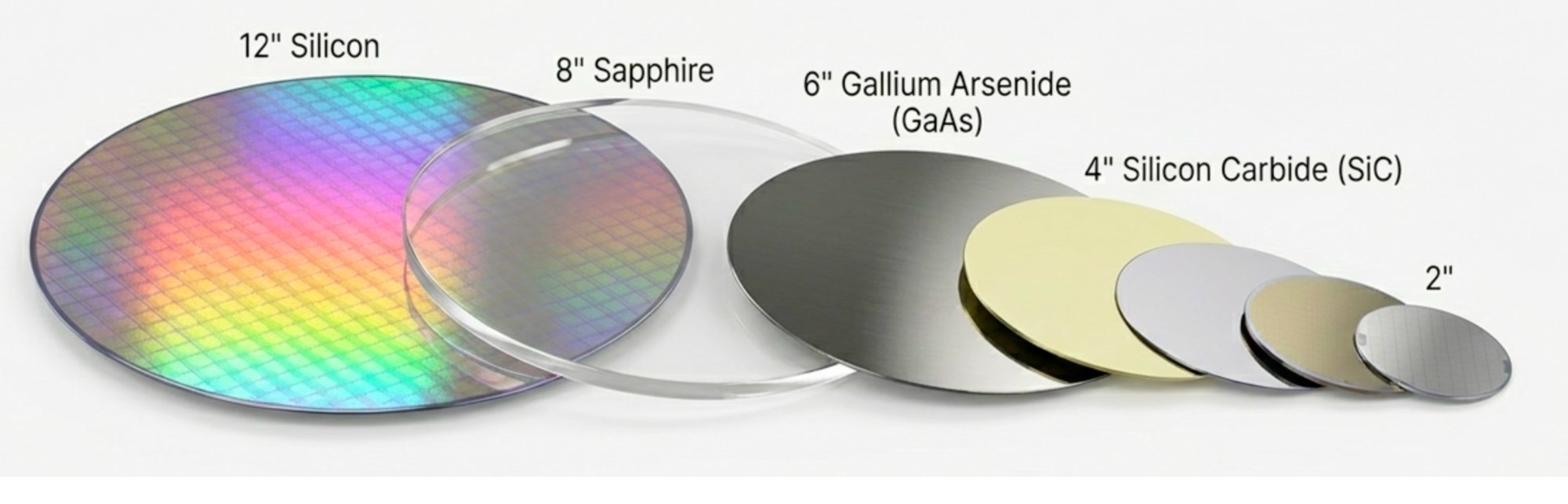
Diameters
Full size range from research to production
2 inch4 inch6 inch
8 inch12 inch
Grade
Three quality tiers for every budget and application
PrimeTestMechanical
Surface Finish
SSP (Single Side Polished)
DSP (Double Side Polished)
Unpolished
Resistivity
Low <0.01 Ω·cm
Medium 1-10 Ω·cm
High >10 Ω·cm
Flatness & Notch
StandardSemi-standardNotched
Coated Silicon Options
THERMAL OXIDE
Wet and dry thermal oxide SiO₂. High-quality gate oxide, isolation, or etch-stop layers. Available on prime wafers.
THIN FILM COATED
Thin film deposited wafers available in lots of 25, 50, and 100 wafers. Custom films on request.
EPITAXIAL SILICON
Epi silicon on heavily doped substrate. N on N+, P on P+. Custom epi specifications on request.