Indium Bump Services
for Cryogenic, IR & Quantum Devices
At Nanosystems JP Inc., we offer wafer-level indium (In) bumping via two complementary routes, thermal evaporation with lift-off patterning and indium electroplating through a resist mold. Pure 4N indium, fine-pitch arrays for focal plane array hybridization, and bumped wafers ready for flip-chip at your facility or chosen assembly site, or in the same program through the flip-chip assembly service, or flip-chip assembly can be included in the same program. Indium stays ductile at millikelvin temperatures and turns superconducting below 3.4 K.
low-temperature solder bump
below ~3.4 K
incl. compound semiconductors
within wafer (evaporated)
Need a hermetic, high-temperature eutectic instead?
Indium is the choice for cryogenic ductility and a particularly low bonding temperature. When the assembly needs a rigid hermetic joint that survives high operating temperatures, eutectic AuSn 80/20 is the standard, see our dedicated AuSn bump page.
Wafer-level indium bump fabrication
for flip-chip hybridization
We fabricate indium bumps on your wafer, thermal evaporation with lift-off or electroplating, delivering a bumped wafer ready for flip-chip hybridization at your facility or chosen assembly site, or in the same program through the flip-chip assembly service. Indium combines three properties especially valuable for cryogenic and IR hybridization: low-temperature compliance, low process temperature, and superconductivity below its transition.
Ductile at Cryogenic Temperatures
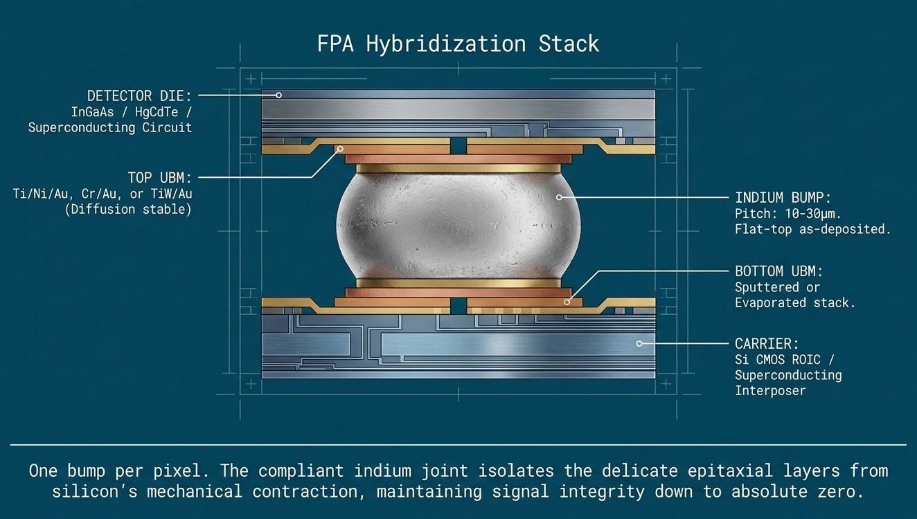
Many conventional solders lose compliance at cryogenic temperatures, while indium keeps unusually high ductility. Indium remains soft and ductile down to millikelvin temperatures, so the bump array absorbs the CTE mismatch between the detector material (HgCdTe, InSb, InGaAs) and the silicon readout circuit through every cool-down cycle. This mechanical compliance is why indium is the universal interconnect for cooled focal plane arrays: more rigid interconnect systems build substantially higher thermomechanical stress over repeated thermal cycles.
Lowest-Temperature Bonding, Even Cold Weld
Indium melts at 156.6 °C, substantially lower than common SnAg and AuSn systems, and freshly prepared indium surfaces cold-weld under pressure at room temperature with no reflow at all. Temperature-sensitive materials, II-VI detector layers, pre-released MEMS, and qubit circuits are never exposed to the 220 to 280 °C excursions that SnAg or AuSn require. Bonding modes: low-temperature reflow, thermocompression, or room-temperature cold-welding.
Superconducting Below 3.4 K
Indium becomes superconducting at 3.4 K. In a dilution refrigerator, indium bump interconnects carry signals between the qubit die and the interposer or carrier with effectively zero DC resistance, with RF performance set by interface quality and assembly design. The same property benefits TES, MKID, and SNSPD readout assemblies operating below 1 K.
Thermal evaporation and electroplating -
matched to your application
Both routes deposit pure indium but use different physics, enabling different trade-offs in pitch, bump height, and throughput. Our engineers recommend the optimal route based on your array geometry, substrate, and bonding method.
Thermal Evaporation + Lift-Off
Indium is thermally evaporated onto a wafer patterned with a lift-off resist profile. Dissolving the resist leaves indium bumps only in the lithographically defined openings, no wet etching of indium is ever required. Because the bump footprint is set by the resist opening, evaporation plus lift-off achieves the finest pitches, the tightest position accuracy, and the best height uniformity. This is the standard route for focal plane array hybridization at 10 to 30 µm pitch and for quantum processor bump arrays.
After lift-off, bumps ship as-deposited, with height and geometry set by deposition and the lift-off pattern.
Indium Electroplating
Indium is electroplated through a photoresist mold onto a sputtered seed layer. After plating, the resist is stripped and the seed layer is etched, leaving freestanding indium bumps. Plating deposits indium far faster than evaporation and builds significantly taller bumps, which matters when the assembly needs large stand-off height for underfill flow, thermal compliance, or non-planar die. The route of choice for larger-pitch arrays, X-ray detector hybrids, and volume runs.
| Parameter | Evaporation + Lift-Off | Electroplating |
|---|---|---|
| Bump height | 2 to 10 µm typical | 5 to 25 µm typical |
| Minimum pitch | 10 µm typical | ~25 µm typical |
| Height uniformity | ±5% within wafer | ±8% within wafer |
| Throughput | Lower (evaporation rate) | Higher (batch plating) |
| Best for | Fine-pitch FPA, quantum | Tall stand-off, volume |
One bump process,
three ways to bond
We fabricate the bumps; hybridization runs at your facility or chosen assembly site, or in the same program through the flip-chip assembly service. Indium gives you three bonding modes from the same bumped wafer, and we tune bump geometry and surface condition to the mode you will use.
same flow, adjusted metallurgy
The indium family extends beyond the pure metal. Selected low-temperature and cryogenic alloy systems can be evaluated by evaporation and lift-off or other suitable routes, with composition control developed per alloy. Quote them through the indium RFQ below.
PbIn: Superconducting Joints
Lead-indium alloys such as In50Pb50 (solidus ~184 °C, liquidus ~209 °C) carry the superconducting heritage of Josephson-era electronics, with transition temperatures near 7 K and mechanical compliance between pure In and pure Pb. Used where a superconducting joint with more strength or a higher melting point than pure indium is specified.
InSn: The 118 °C Eutectic
In52Sn48 is a 118 °C eutectic option for assemblies that require a lower reflow than pure indium (157 °C) or SnAg. The joint stays compliant at cryogenic temperature, serving low-temperature photonics, temperature-limited sensors, and step-soldering hierarchies under pure indium.
InAg: Strengthened Indium
In-Ag low-temperature alloys add silver's strengthening (including AgIn intermetallic phases) to indium's ductility, improving creep resistance and joint strength while keeping the melting point below 157 °C and the cryogenic compliance intact. Compositions are confirmed in wt% for each program. The choice when pure indium joints are mechanically marginal.
Sn & BiSn: The Lowest Rungs
Plain evaporated tin for standard-solder compatibility on the same lift-off flow, and Bi58Sn42, the 139°C eutectic, for joins where even 157°C is too hot: polymer-bearing MEMS, temperature-fragile optics, and already-populated stacks that cannot see another full reflow. Pure Bi (271°C) available for special cases.
the films beside the bumps
Superconducting qubit and detector flows pair indium bumps with superconducting thin films, and both use the same lift-off discipline. We deposit and pattern the films alongside the bumps in one program.
Films, Pads & Resonator Metal
Evaporated niobium, aluminum, and Ti/Au patterned by lift-off for cryogenic circuits: resonators, ground planes, wiring layers, and the pads indium bumps land on. Deposited with the same interface discipline as our contact stacks, one pump-down, in-situ pre-clean, and delivered next to the bump lithography they must align to.
Josephson-Adjacent: Dolan Bridge
The most specialized version of this discipline is double-angle aluminum evaporation through a suspended resist bridge with controlled in-situ oxidation between the two depositions, the Dolan bridge process behind Josephson junctions. It is the same lift-off logic; junction programs are taken by arrangement, so bring your specs to the RFQ. The companion low-temperature joint is Au/In SLID, on the same flow.
Lift-off definition and
native oxide management
Two things separate indium bumping that hybridizes reliably from indium bumping that does not: geometry control without etching, and control of the native oxide between our deposition and your bonder.
Lift-Off, No Undercut
A photoresist layer is patterned by lithography before any metal deposition. Indium is then evaporated over the entire wafer, and dissolving the resist carries away the metal on top of it, leaving bumps only in the defined openings. No acid ever contacts the bump surface, so there is no undercut and no purity loss. Bump width, spacing, and alignment to the underlying pads are controlled by lithographic registration at ±0.5 µm.
Native Oxide Under Control
Indium grows a thin native oxide within minutes of air exposure, and that oxide skin is what makes or breaks cold-weld and thermocompression bonding. The interval between lift-off and packing is controlled and recorded, and wafers are sealed in a moisture barrier bag with desiccant and a humidity indicator card, inside a rigid wafer shipper. Bumps arrive at your bonder in a known and documented surface state. Time-out guidance and bonding-side treatment recommendations are provided for your reflow, thermocompression, or cold-weld process.
Uniformity Across the Array
A focal plane array hybridizes correctly only if every bump in the array touches down together. Bump height is mapped by profilometry across the wafer, with ±5% within-wafer uniformity on the evaporation route, and bump geometry is verified by SEM before shipment. Height maps and SEM images are delivered with the wafers as standard process data, so your bonding engineers start from measured reality, not assumptions.
Detector, ROIC, and
compound semiconductor wafers
IR and quantum work rarely happens on plain silicon. Indium bumping runs on CMOS readout wafers, compound semiconductors, and fragile thinned substrates, with handling and thermal budgets adapted to each.
ROIC and Detector Wafers
Readout wafers arrive with completed CMOS and strict thermal ceilings; detector wafers carry epitaxial layers that tolerate even less. Every run is processed against a written thermal budget agreed before the run starts, with UBM and deposition conditions selected to stay inside it. Bump arrays are aligned to your existing pad layout at ±0.5 µm stepper registration, matched die by die to the array you will hybridize.
Compound, Thin, and Fragile Substrates
InP and GaAs wafers, glass and sapphire carriers, and thinned or bowed wafers are handled with adapted chucking, coating, and transport. Substrate-specific resist processes planarize over topography, and deposition conditions are tuned for step coverage where the layout demands it. If your substrate is unusual, send the details, unusual substrates are the normal case in this application space.
Complete indium bump
fabrication parameters
| Parameter | Evaporation + Lift-Off | Electroplating |
|---|---|---|
| Wafer Sizes | 4 to 12 inch (100 to 300 mm) | |
| Substrates | Si, CMOS ROIC wafers, InP, GaAs, glass, sapphire; others on request | |
| Primary Material | Indium (In), 99.99% (4N) purity standard | |
| UBM Options | Ti/Ni/Au, Cr/Au, TiW/Au; ENIG-finished pads accepted | |
| Bump Height | 2 to 10 µm typical | 5 to 25 µm typical |
| Minimum Pitch | 10 µm typical, finer on request | ~25 µm typical |
| Array Size | Up to full-wafer arrays, megapixel-class bump counts per die | |
| Height Uniformity | ±5% within-wafer | ±8% within-wafer |
| Patterning Method | Lift-off | Through-resist plating + seed etch |
| Lithography | stepper and mask aligner | stepper and mask aligner |
| Alignment Accuracy | ±0.5 µm (stepper) | ±1 µm |
| Bonding Compatibility | Reflow (above 156.6 °C), thermocompression, room-temperature cold-weld | |
| Melting Point (pure In) | 156.6 °C | |
| Superconducting Tc | 3.4 K | |
| Thermal Conductivity (In) | ~82 W/m·K near room temperature | |
| Inspection | Profilometry height map + SEM standard; bump shear test on request | |
| Shipment | Nitrogen-sealed with handling and time-out guidance | |
Indium bumps across IR, quantum,
and scientific instrumentation
IR Focal Plane Array Hybridization
Flip-chip hybridization of InGaAs, InSb, HgCdTe, and type-II superlattice detector arrays onto silicon readout integrated circuits (ROIC). Fine-pitch indium bump arrays at 10 to 30 µm pitch enable megapixel-class focal planes for thermal imaging, astronomy, and space instruments, with the ductile indium joint absorbing detector-to-silicon CTE mismatch through every cool-down.
Superconducting Quantum Processors
Indium bump flip-chip is the established architecture for connecting the qubit die to the interposer or carrier chip in superconducting quantum computers. Below its 3.4 K transition, indium carries signals with zero DC resistance, and cold-weld or low-temperature bonding keeps the fragile Josephson junction circuits far below damaging temperatures during assembly.
Cryogenic Detectors & Instruments
TES bolometers, MKID arrays, and SNSPD assemblies operating below 1 K rely on indium interconnects that stay ductile and superconducting at operating temperature. Indium bump hybridization connects large detector arrays to multiplexed readout in CMB instruments, sub-mm astronomy, and dark matter experiments.
X-ray & Particle Pixel Detectors
Hybrid pixel detectors bond CdTe, CZT, GaAs, or thick silicon sensor die to readout ASICs bump by bump. Taller plated indium bumps provide the stand-off and compliance these large-area hybrids need, serving photon-counting medical CT, synchrotron science, and high-energy physics trackers.
SWIR Imaging & LiDAR Receivers
InGaAs SWIR cameras for machine vision, semiconductor inspection, and eye-safe LiDAR receivers use indium bump hybridization between the photodiode array and the silicon readout. Growing automotive and industrial SWIR volumes are pushing pitch and array size, both strengths of the evaporation lift-off route.
Low-Temperature Photonic Die Attach
When a laser, modulator, or detector die cannot tolerate the reflow temperature of SnAg or AuSn, indium bonds at 156.6 °C or below. Used for temperature-sensitive III-V die, micro-LED and micro-optic assembly, and rework-tolerant prototype photonic packages.
Low-Temperature Hermetic & Vacuum Sealing
Indium seal rings and gaskets can provide hermetic, vacuum-compatible seals when properly designed and compressed as a particularly low-temperature metallic sealing option, for cryostat windows, MEMS vacuum packages, and optical assemblies where organic seals outgas or crack at cryogenic temperature.
Fine-Pitch 3D Stacking & Chiplet R&D
Indium micro-bumps are an active research direction for ultra-fine-pitch die stacking and chiplet interconnects, bonding at low temperature with high compliance. We support university and corporate R&D programs with prototype indium micro-bump wafers from a single wafer per run.
What makes our indium bump capability
different
Two deposition routes, one recommendation
Thermal evaporation with lift-off and indium electroplating are both available. Our engineers select the route that fits your pitch, bump height, substrate, and volume, so you are not limited to a single route.
UBM included, matched to your pads
Ti/Ni/Au, Cr/Au, or TiW/Au under-bump metallization is deposited and patterned as part of the same flow, matched to your pad finish and your bonding method, so the wafer arrives genuinely ready to hybridize.
Fine pitch by lift-off, no undercut
Bump footprint is defined by the resist opening at ±0.5 µm stepper registration. No etch ever contacts the indium, so there is no undercut and no purity loss, the geometry that fine-pitch focal plane arrays demand.
Oxide-aware from deposition to your bonder
Indium bonding succeeds or fails on surface condition. Wafers ship in sealed moisture-barrier bags with desiccant and a humidity indicator card, with documented time-out and bonding-side preparation guidance for reflow, thermocompression, or cold-weld assembly.
Cryo and quantum context understood
CTE compliance across a 300 K cool-down, superconducting interconnect requirements, thermal budgets for Josephson junction circuits and II-VI detector layers: the bump array is engineered as part of your cryogenic assembly, not as an isolated deposition job.
From 1 wafer, no minimum lot
Prototype indium bumping on a single wafer, verify height uniformity, geometry, and bonding behavior before committing to volume. The prototype data becomes the baseline for repeat production on the same recipe.
Start your project.
Initial response typically within one business day.
Share your process requirements, substrate, and production volume. A Nanosystems JP Inc. engineer will give an initial response typically within one business day. Full quote typically within 7-10 business days, subject to project complexity and NDA requirements.